Chem
-
 Ultra-Low Power Flexible Memory Using 2D Materials
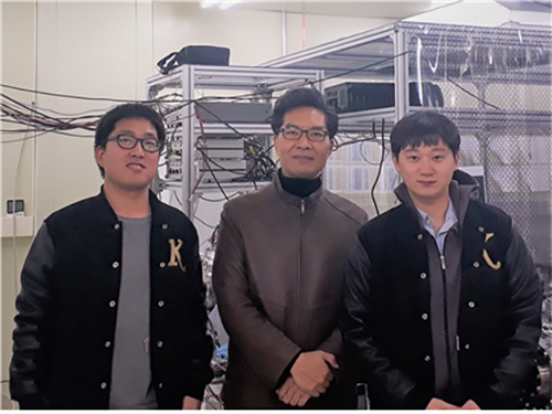
(Professor Choi and Ph.D. candidate Jang)
KAIST research team led by Professor Sung-Yool Choi at School of Electrical Engineering and Professor Sung Gap Im at the Department of Chemical and Biomolecular Engineering developed high-density, ultra-low power, non-volatile, flexible memory technology using 2D materials. The team used ultrathin molybdenum disulfide (MoS2) with atomic-scale thickness as the channel material and high-performance polymeric insulator film as the tunneling dielectric material. This research was published on the cover of Advanced Functional Materials on November 17. KAIST graduate Myung Hun Woo, a researcher at Samsung Electronics and Ph.D. candidate Byung Chul Jang are first authors.
The surge of new technologies such as Internet of Things (IoT), Artificial Intelligence (AI), and cloud server led to the paradigm shift from processor-centric computing to memory-centric computing in the industry, as well as the increase in demand of wearable devices. This led to an increased need for high-density, ultra-low power, non-volatile flexible memory. In particular, ultrathin MoS2 as semiconductor material has been recently regarded as post-silicon material. This is due to its ultrathin thickness of atomic-scale which suppresses short channel effect observed in conventional silicon material, leading to advantages in high- density and low-power consumption. Further, this thickness allows the material to be flexible, and thus the material is applicable to wearable devices.
However, due to the dangling-bond free surface of MoS2 semiconductor material, it is difficult to deposit the thin insulator film to be uniform and stable over a large area via the conventional atomic layer deposition process. Further, the currently used solution process makes it difficult to deposit uniformly low dielectric constant (k) polymeric insulator film with sub-10 nm thickness on a large area, thus indicating that the memory device utilizing the conventional solution-processed polymer insulator film cannot be operated at low-operating voltage and is not compatible with photolithography.
The research team tried to overcome the hurdles and develop high-density, ultra-low power, non-volatile flexible memory by employing a low-temperature, solvent-free, and all-dry vapor phase technique named initiated chemical vapor deposition (iCVD) process. Using iCVD process, tunneling polymeric insulator film with 10 nm thickness was deposited uniformly on MoS2 semiconductor material without being restricted by the dangling bond-free surface of MoS2. The team observed that the newly developed MoS2-based non-volatile memory can be operated at low-voltage (around 10V), in contrast to the conventional MoS2-based non-volatile memory that requires over 20V.
Professor Choi said, “As the basis for the Fourth Industrial revolution technologies including AI and IoT, semiconductor device technology needs to have characteristics of low-power and flexibility, in clear contrast to conventional memory devices.” He continued, “This new technology is significant in developing source technology in terms of materials, processes, and devices to contribute to achieve these characteristics.”
This research was supported by the Global Frontier Center for Advanced Soft Electronics and the Creative Materials Discovery Program by funded the National Research Foundation of Korea of Ministry of Science and ICT.
( Figure 1. Cover of Advanced Functional Materials)
(Figure 2. Concept map for the developed non-volatile memory material and high-resolution transmission electron microscopy image for material cross-section )
2018.01.02 View 10153
Ultra-Low Power Flexible Memory Using 2D Materials
(Professor Choi and Ph.D. candidate Jang)
KAIST research team led by Professor Sung-Yool Choi at School of Electrical Engineering and Professor Sung Gap Im at the Department of Chemical and Biomolecular Engineering developed high-density, ultra-low power, non-volatile, flexible memory technology using 2D materials. The team used ultrathin molybdenum disulfide (MoS2) with atomic-scale thickness as the channel material and high-performance polymeric insulator film as the tunneling dielectric material. This research was published on the cover of Advanced Functional Materials on November 17. KAIST graduate Myung Hun Woo, a researcher at Samsung Electronics and Ph.D. candidate Byung Chul Jang are first authors.
The surge of new technologies such as Internet of Things (IoT), Artificial Intelligence (AI), and cloud server led to the paradigm shift from processor-centric computing to memory-centric computing in the industry, as well as the increase in demand of wearable devices. This led to an increased need for high-density, ultra-low power, non-volatile flexible memory. In particular, ultrathin MoS2 as semiconductor material has been recently regarded as post-silicon material. This is due to its ultrathin thickness of atomic-scale which suppresses short channel effect observed in conventional silicon material, leading to advantages in high- density and low-power consumption. Further, this thickness allows the material to be flexible, and thus the material is applicable to wearable devices.
However, due to the dangling-bond free surface of MoS2 semiconductor material, it is difficult to deposit the thin insulator film to be uniform and stable over a large area via the conventional atomic layer deposition process. Further, the currently used solution process makes it difficult to deposit uniformly low dielectric constant (k) polymeric insulator film with sub-10 nm thickness on a large area, thus indicating that the memory device utilizing the conventional solution-processed polymer insulator film cannot be operated at low-operating voltage and is not compatible with photolithography.
The research team tried to overcome the hurdles and develop high-density, ultra-low power, non-volatile flexible memory by employing a low-temperature, solvent-free, and all-dry vapor phase technique named initiated chemical vapor deposition (iCVD) process. Using iCVD process, tunneling polymeric insulator film with 10 nm thickness was deposited uniformly on MoS2 semiconductor material without being restricted by the dangling bond-free surface of MoS2. The team observed that the newly developed MoS2-based non-volatile memory can be operated at low-voltage (around 10V), in contrast to the conventional MoS2-based non-volatile memory that requires over 20V.
Professor Choi said, “As the basis for the Fourth Industrial revolution technologies including AI and IoT, semiconductor device technology needs to have characteristics of low-power and flexibility, in clear contrast to conventional memory devices.” He continued, “This new technology is significant in developing source technology in terms of materials, processes, and devices to contribute to achieve these characteristics.”
This research was supported by the Global Frontier Center for Advanced Soft Electronics and the Creative Materials Discovery Program by funded the National Research Foundation of Korea of Ministry of Science and ICT.
( Figure 1. Cover of Advanced Functional Materials)
(Figure 2. Concept map for the developed non-volatile memory material and high-resolution transmission electron microscopy image for material cross-section )
2018.01.02 View 10153 -
 Non-Adiabatic Reaction Mechanism Identified at Conical Intersection
(Professor Kim(center) and Ph.D. candidates Kyung Chul Woo (left) and Kang Do Hyung)
Research team led by Professor Sang Kyu Kim at KAIST Department of Chemistry observed two distinct reaction pathways that occur at conical intersection where two different adiabatic potential energy surfaces cross at the same nuclear configuration.
Professor Kim previously identified the existence and molecular structure of conical intersection in 2010. In this following study, the team accurately measured reaction rates of two totally different reaction pathways activated only at conical intersection where the seminal Born-Oppenheimer approximation breaks down.
This study led by Kyung Chul Woo (1st author) and Do Hyung Kang, both Ph.D. candidates at KAIST, was published in Journal of the American Chemical Society in November 7th, 2017.
Chemical reaction induced by light occurs in excited electronic states where the reaction outcome is often destined by coupling among different electronic states mediated by nuclear motions during chemical reaction. Such a coupling is most critical and important at the conical intersection as nonadiabtic surface-hopping is most probable at situation where the Born-Oppenheimer approximation fails.
Professor Kim used spectroscopic methods in 2010 to experimentally observe conical intersection of polyatomic molecule. And yet, it was not possible to disentangle complex dynamic processes with frequency-domain study only.
The research team used pico-second time-resolution kinetic energy resolved mass spectrometry to identify two possible distinct reaction pathways in both energy and time domains.,.
The research team demonstrated that the reactive flux prepared at the conical intersection is bifurcated into adiabatic or non-adiabatic reaction pathways. These two pathways are quite distinct in terms of reaction rates, energy releases, and product branching ratios.
This is the first study to capture the moment of bifurcation dynamics at the conical intersection for complex polyatomic molecular system. The study could contribute to conceptual improvement in understanding complicated nonadiabatic dynamics in general.
Professor Kim said, “Basic science research is essential in understanding and wisely using the nature. New technological advances cannot be made without the advancement in basic science.” He continued, “I hope this study could lead to growth in many young academic talents in basic sciences.”
(Figure 1. Reaction graph starting from reaction intersection that divides into adiabatic reaction pathway (red) and non-adiabatic pathway (blue))
2017.12.19 View 6795
Non-Adiabatic Reaction Mechanism Identified at Conical Intersection
(Professor Kim(center) and Ph.D. candidates Kyung Chul Woo (left) and Kang Do Hyung)
Research team led by Professor Sang Kyu Kim at KAIST Department of Chemistry observed two distinct reaction pathways that occur at conical intersection where two different adiabatic potential energy surfaces cross at the same nuclear configuration.
Professor Kim previously identified the existence and molecular structure of conical intersection in 2010. In this following study, the team accurately measured reaction rates of two totally different reaction pathways activated only at conical intersection where the seminal Born-Oppenheimer approximation breaks down.
This study led by Kyung Chul Woo (1st author) and Do Hyung Kang, both Ph.D. candidates at KAIST, was published in Journal of the American Chemical Society in November 7th, 2017.
Chemical reaction induced by light occurs in excited electronic states where the reaction outcome is often destined by coupling among different electronic states mediated by nuclear motions during chemical reaction. Such a coupling is most critical and important at the conical intersection as nonadiabtic surface-hopping is most probable at situation where the Born-Oppenheimer approximation fails.
Professor Kim used spectroscopic methods in 2010 to experimentally observe conical intersection of polyatomic molecule. And yet, it was not possible to disentangle complex dynamic processes with frequency-domain study only.
The research team used pico-second time-resolution kinetic energy resolved mass spectrometry to identify two possible distinct reaction pathways in both energy and time domains.,.
The research team demonstrated that the reactive flux prepared at the conical intersection is bifurcated into adiabatic or non-adiabatic reaction pathways. These two pathways are quite distinct in terms of reaction rates, energy releases, and product branching ratios.
This is the first study to capture the moment of bifurcation dynamics at the conical intersection for complex polyatomic molecular system. The study could contribute to conceptual improvement in understanding complicated nonadiabatic dynamics in general.
Professor Kim said, “Basic science research is essential in understanding and wisely using the nature. New technological advances cannot be made without the advancement in basic science.” He continued, “I hope this study could lead to growth in many young academic talents in basic sciences.”
(Figure 1. Reaction graph starting from reaction intersection that divides into adiabatic reaction pathway (red) and non-adiabatic pathway (blue))
2017.12.19 View 6795 -
 Technology Detecting RNase Activity
(Ph.D. candidate Chang Yeol Lee)
A KAIST research team of Professor Hyun Gyu Park at Department of Chemical and Biomolecular Engineering developed a new technology to detect the activity of RNase H, a RNA degrading enzyme. The team used highly efficient signal amplification reaction termed catalytic hairpin assembly (CHA) to effectively analyze the RNase H activity. Considering that RNase H is required in the proliferation of retroviruses such as HIV, this research finding could contribute to AIDS treatments in the future, researchers say.
This study led by Ph.D. candidates Chang Yeol Lee and Hyowon Jang was chosen as the cover for Nanoscale (Issue 42, 2017) published in 14 November.
The existing techniques to detect RNase H require expensive fluorophore and quencher, and involve complex implementation. Further, there is no way to amplify the signal, leading to low detection efficiency overall. The team utilized CHA technology to overcome these limitations. CHA amplifies detection signal to allow more sensitive RNase H activity assay.
The team designed the reaction system so that the product of CHA reaction has G-quadruplex structures, which is suitable to generate fluorescence. By using fluorescent molecules that bind to G-quadruplexes to generate strong fluorescence, the team could develop high performance RNase H detection method that overcomes the limitations of existing techniques. Further, this technology could screen inhibitors of RNase H activity.
The team expects that the research finding could contribute to AIDS treatment. AIDS is disease caused by HIV, a retrovirus that utilizes reverse transcription, during which RNA is converted to DNA. RNase H is essential for reverse transcription in HIV, and thus inhibition of RNase H could in turn inhibit transcription of HIV DNA.
Professor Park said, “This technology is applicable to detect various enzyme activities, as well as RNase H activity.” He continued, “I hope this technology could be widely used in research on enzyme related diseases.”
This study was funded by Global Frontier project and Mid-career Researcher Support project of the Ministry of Science and ICT.
2017.11.28 View 7317
Technology Detecting RNase Activity
(Ph.D. candidate Chang Yeol Lee)
A KAIST research team of Professor Hyun Gyu Park at Department of Chemical and Biomolecular Engineering developed a new technology to detect the activity of RNase H, a RNA degrading enzyme. The team used highly efficient signal amplification reaction termed catalytic hairpin assembly (CHA) to effectively analyze the RNase H activity. Considering that RNase H is required in the proliferation of retroviruses such as HIV, this research finding could contribute to AIDS treatments in the future, researchers say.
This study led by Ph.D. candidates Chang Yeol Lee and Hyowon Jang was chosen as the cover for Nanoscale (Issue 42, 2017) published in 14 November.
The existing techniques to detect RNase H require expensive fluorophore and quencher, and involve complex implementation. Further, there is no way to amplify the signal, leading to low detection efficiency overall. The team utilized CHA technology to overcome these limitations. CHA amplifies detection signal to allow more sensitive RNase H activity assay.
The team designed the reaction system so that the product of CHA reaction has G-quadruplex structures, which is suitable to generate fluorescence. By using fluorescent molecules that bind to G-quadruplexes to generate strong fluorescence, the team could develop high performance RNase H detection method that overcomes the limitations of existing techniques. Further, this technology could screen inhibitors of RNase H activity.
The team expects that the research finding could contribute to AIDS treatment. AIDS is disease caused by HIV, a retrovirus that utilizes reverse transcription, during which RNA is converted to DNA. RNase H is essential for reverse transcription in HIV, and thus inhibition of RNase H could in turn inhibit transcription of HIV DNA.
Professor Park said, “This technology is applicable to detect various enzyme activities, as well as RNase H activity.” He continued, “I hope this technology could be widely used in research on enzyme related diseases.”
This study was funded by Global Frontier project and Mid-career Researcher Support project of the Ministry of Science and ICT.
2017.11.28 View 7317 -
 Dr. Steven Chu Talks on Sustainable Energy Policy at KAIST
Nobel Laureate in physics and former US Energy Secretary Steven Chu called for concerted efforts to develop a more sustainable energy policy and portfolio at a lecture held at KAIST and a forum in Seoul on November 23.
A policy with an energy mix including nuclear power and renewable energy could be ideal for retaining a stable energy supply given Korea’s very limited geographical conditions, Chu said during the Future Energy Forum in Seoul. He also held a lecture at KAIST’s Daejeon campus on “Climate Change, the Importance of Science and Policy in Achieving a Sustainable Future.”
He said that unlike the United States, Korea and Japan have geographical limitations for generating enough renewable energy. "Wind speeds of more than 10 meters per second would allow wind power generation, but, South Korea's southernmost wind speed in Jeju is less than 8 meters per second, and the amount of sunshine is lower than in the Middle East. It is ideal to combine renewable energy with nuclear power plants," he said.
Chu also stressed the role of science in achieving a sustainable future, citing many cases in foreign countries. For instance, Germany once decided to do away with nuclear power. However, their initial plan does not directly raise energy efficiency and the proportion of fossil fuels has led to an increase in the environmental issue of fine particular matter as well as carbon dioxide emission increases.
He said that in the long term, renewable energy will emerge as major alternative resources, stressing the role of science in achieving a sustainable future. Without this alternative, we will eventually burn more fossil fuels and pollute the air.
Chu also said that nuclear waste and safe plant operation will be a big concern, but it is technologically viable since Korea has already proven its prowess in nuclear power plant building and safety technology.
Chu added, "Research in chemical energy storage through novel electrochemistry may lead to solutions, but for the next half century we will need additional energy-on-demand and carbon-free sources of energy from proven technologies."
"While science, innovation and technology will no doubt lead to better solutions, sound government policies are needed to advance the transition to carbon-free energy needed to achieve a more sustainable world," he said.
After serving as the US Secretary of Energy for four years from 2009 to 2013, Professor Chu returned to Stanford University, and currently holds a position of the William R. Kenan, Jr. Professor of Physics as well as Professor in the Department of Molecular and Cellular Physiology.
Professor Chu is known for his research at Bell Labs and Stanford University regarding the cooling and trapping of atoms with laser light, for which he won the Nobel Prize in Physics in 1997.
2017.11.24 View 5451
Dr. Steven Chu Talks on Sustainable Energy Policy at KAIST
Nobel Laureate in physics and former US Energy Secretary Steven Chu called for concerted efforts to develop a more sustainable energy policy and portfolio at a lecture held at KAIST and a forum in Seoul on November 23.
A policy with an energy mix including nuclear power and renewable energy could be ideal for retaining a stable energy supply given Korea’s very limited geographical conditions, Chu said during the Future Energy Forum in Seoul. He also held a lecture at KAIST’s Daejeon campus on “Climate Change, the Importance of Science and Policy in Achieving a Sustainable Future.”
He said that unlike the United States, Korea and Japan have geographical limitations for generating enough renewable energy. "Wind speeds of more than 10 meters per second would allow wind power generation, but, South Korea's southernmost wind speed in Jeju is less than 8 meters per second, and the amount of sunshine is lower than in the Middle East. It is ideal to combine renewable energy with nuclear power plants," he said.
Chu also stressed the role of science in achieving a sustainable future, citing many cases in foreign countries. For instance, Germany once decided to do away with nuclear power. However, their initial plan does not directly raise energy efficiency and the proportion of fossil fuels has led to an increase in the environmental issue of fine particular matter as well as carbon dioxide emission increases.
He said that in the long term, renewable energy will emerge as major alternative resources, stressing the role of science in achieving a sustainable future. Without this alternative, we will eventually burn more fossil fuels and pollute the air.
Chu also said that nuclear waste and safe plant operation will be a big concern, but it is technologically viable since Korea has already proven its prowess in nuclear power plant building and safety technology.
Chu added, "Research in chemical energy storage through novel electrochemistry may lead to solutions, but for the next half century we will need additional energy-on-demand and carbon-free sources of energy from proven technologies."
"While science, innovation and technology will no doubt lead to better solutions, sound government policies are needed to advance the transition to carbon-free energy needed to achieve a more sustainable world," he said.
After serving as the US Secretary of Energy for four years from 2009 to 2013, Professor Chu returned to Stanford University, and currently holds a position of the William R. Kenan, Jr. Professor of Physics as well as Professor in the Department of Molecular and Cellular Physiology.
Professor Chu is known for his research at Bell Labs and Stanford University regarding the cooling and trapping of atoms with laser light, for which he won the Nobel Prize in Physics in 1997.
2017.11.24 View 5451 -
 Ultra-Fast and Ultra-Sensitive Hydrogen Sensor
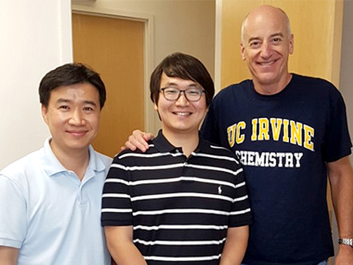
(From left: Professor Kim, Ph.D. candidate Koo, and Professor Penner)
A KAIST team made an ultra-fast hydrogen sensor that can detect hydrogen gas levels under 1% in less than seven seconds. The sensor also can detect hundreds of parts per million levels of hydrogen gas within 60 seconds at room temperature.
A research group under Professor Il-Doo Kim in the Department of Materials Science and Engineering at KAIST, in collaboration with Professor Reginald M. Penner of the University of California-Irvine, has developed an ultra-fast hydrogen gas detection system based on a palladium (Pd) nanowire array coated with a metal-organic framework (MOF).
Hydrogen has been regarded as an eco-friendly next-generation energy source. However, it is a flammable gas that can explode even with a small spark. For safety, the lower explosion limit for hydrogen gas is 4 vol% so sensors should be able to detect the colorless and odorless hydrogen molecule quickly. The importance of sensors capable of rapidly detecting colorless and odorless hydrogen gas has been emphasized in recent guidelines issued by the U.S. Department of Energy. According to the guidelines, hydrogen sensors should detect 1 vol% of hydrogen in air in less than 60 seconds for adequate response and recovery times.
To overcome the limitations of Pd-based hydrogen sensors, the research team introduced a MOF layer on top of a Pd nanowire array. Lithographically patterned Pd nanowires were simply overcoated with a Zn-based zeolite imidazole framework (ZIF-8) layer composed of Zn ions and organic ligands. ZIF-8 film is easily coated on Pd nanowires by simple dipping (for 2–6 hours) in a methanol solution including Zn (NO3)2·6H2O and 2-methylimidazole.
(This cover image depicts lithographically-patterned Pd nanowires overcoated with a Zn-based zeolite imidazole framework (ZIF-8) layer.)
As synthesized ZIF-8 is a highly porous material composed of a number of micro-pores of 0.34 nm and 1.16 nm, hydrogen gas with a kinetic diameter of 0.289 nm can easily penetrate inside the ZIF-8 membrane, while large molecules (> 0.34 nm) are effectively screened by the MOF filter. Thus, the ZIF-8 filter on the Pd nanowires allows the predominant penetration of hydrogen molecules, leading to the acceleration of Pd-based H2 sensors with a 20-fold faster recovery and response speed compared to pristine Pd nanowires at room temperature.
Professor Kim expects that the ultra-fast hydrogen sensor can be useful for the prevention of explosion accidents caused by the leakage of hydrogen gas. In addition, he expects that other harmful gases in the air can be accurately detected through effective nano-filtration by using of a variety of MOF layers.
This study was carried out by Ph.D. candidate Won-Tae Koo (first author), Professor Kim (co-corresponding author), and Professor Penner (co-corresponding author). The study has been published in the online edition of ACS Nano, as the cover-featured image for the September issue.
Figure 1. Representative image for this paper published in ACS Nano, August, 18.
Figure 2. Images of Pd nanowire array-based hydrogen sensors, scanning electron microscopy image of a Pd nanowire covered by a metal-organic framework layer, and the hydrogen sensing properties of the sensors.
Figure 3. Schematic illustration of a metal-organic framework (MOF). The MOF, consisting of metal ions and organic ligands, is a highly porous material with an ultrahigh surface area. The various structures of MOFs can be synthesized depending on the kinds of metal ions and organic ligands.
2017.09.28 View 11522
Ultra-Fast and Ultra-Sensitive Hydrogen Sensor
(From left: Professor Kim, Ph.D. candidate Koo, and Professor Penner)
A KAIST team made an ultra-fast hydrogen sensor that can detect hydrogen gas levels under 1% in less than seven seconds. The sensor also can detect hundreds of parts per million levels of hydrogen gas within 60 seconds at room temperature.
A research group under Professor Il-Doo Kim in the Department of Materials Science and Engineering at KAIST, in collaboration with Professor Reginald M. Penner of the University of California-Irvine, has developed an ultra-fast hydrogen gas detection system based on a palladium (Pd) nanowire array coated with a metal-organic framework (MOF).
Hydrogen has been regarded as an eco-friendly next-generation energy source. However, it is a flammable gas that can explode even with a small spark. For safety, the lower explosion limit for hydrogen gas is 4 vol% so sensors should be able to detect the colorless and odorless hydrogen molecule quickly. The importance of sensors capable of rapidly detecting colorless and odorless hydrogen gas has been emphasized in recent guidelines issued by the U.S. Department of Energy. According to the guidelines, hydrogen sensors should detect 1 vol% of hydrogen in air in less than 60 seconds for adequate response and recovery times.
To overcome the limitations of Pd-based hydrogen sensors, the research team introduced a MOF layer on top of a Pd nanowire array. Lithographically patterned Pd nanowires were simply overcoated with a Zn-based zeolite imidazole framework (ZIF-8) layer composed of Zn ions and organic ligands. ZIF-8 film is easily coated on Pd nanowires by simple dipping (for 2–6 hours) in a methanol solution including Zn (NO3)2·6H2O and 2-methylimidazole.
(This cover image depicts lithographically-patterned Pd nanowires overcoated with a Zn-based zeolite imidazole framework (ZIF-8) layer.)
As synthesized ZIF-8 is a highly porous material composed of a number of micro-pores of 0.34 nm and 1.16 nm, hydrogen gas with a kinetic diameter of 0.289 nm can easily penetrate inside the ZIF-8 membrane, while large molecules (> 0.34 nm) are effectively screened by the MOF filter. Thus, the ZIF-8 filter on the Pd nanowires allows the predominant penetration of hydrogen molecules, leading to the acceleration of Pd-based H2 sensors with a 20-fold faster recovery and response speed compared to pristine Pd nanowires at room temperature.
Professor Kim expects that the ultra-fast hydrogen sensor can be useful for the prevention of explosion accidents caused by the leakage of hydrogen gas. In addition, he expects that other harmful gases in the air can be accurately detected through effective nano-filtration by using of a variety of MOF layers.
This study was carried out by Ph.D. candidate Won-Tae Koo (first author), Professor Kim (co-corresponding author), and Professor Penner (co-corresponding author). The study has been published in the online edition of ACS Nano, as the cover-featured image for the September issue.
Figure 1. Representative image for this paper published in ACS Nano, August, 18.
Figure 2. Images of Pd nanowire array-based hydrogen sensors, scanning electron microscopy image of a Pd nanowire covered by a metal-organic framework layer, and the hydrogen sensing properties of the sensors.
Figure 3. Schematic illustration of a metal-organic framework (MOF). The MOF, consisting of metal ions and organic ligands, is a highly porous material with an ultrahigh surface area. The various structures of MOFs can be synthesized depending on the kinds of metal ions and organic ligands.
2017.09.28 View 11522 -
 A Novel and Practical Fab-route for Superomniphobic Liquid-free Surfaces
(clockwise from left: Jaeho Choi, Hee Tak Kim, Shin-Hyun Kim)
A joint research team led by Professor Hee Tak Kim and Shin-Hyun Kim in the Department of Chemical and Biomolecular Engineering at KAIST developed a fabrication technology that can inexpensively produce surfaces capable of repelling liquids, including water and oil.
The team used the photofluidization of azobenzene molecule-containing polymers to generate a superomniphobic surface which can be applied for developing stain-free fabrics, non-biofouling medical tubing, and corrosion-free surfaces.
Mushroom-shaped surface textures, also called doubly re-entrant structures, are known to be the most effective surface structure that enhances resistance against liquid invasion, thereby exhibiting superior superomniphobic property.
However, the existing procedures for their fabrication are highly delicate, time-consuming, and costly. Moreover, the materials required for the fabrication are restricted to an inflexible and expensive silicon wafer, which limits the practical use of the surface.
To overcome such limitations, the research team used a different approach to fabricate the re-entrant structures called localized photofludization by using the peculiar optical phenomenon of azobenzene molecule-containing polymers (referred to as azopolymers). It is a phenomenon where an azopolymer becomes fluidized under irradiation, and the fluidization takes place locally within the thin surface layer of the azopolymer.
With this novel approach, the team facilitated the localized photofluidization in the top surface layer of azopolymer cylindrical posts, successfully reconfiguring the cylindrical posts to doubly re-entrant geometry while the fluidized thin top surface of an azopolymer is flowing down.
The structure developed by the team exhibits a superior superomniphobic property even for liquids infiltrating the surface immediately.
Moreover, the superomniphobic property can be maintained on a curved target surface because its surficial materials are based on high molecules.
Furthermore, the fabrication procedure of the structure is highly reproducible and scalable, providing a practical route to creating robust omniphobic surfaces.
Professor Hee Tak Kim said, “Not only does the novel photo-fluidization technology in this study produce superior superomniphobic surfaces, but it also possesses many practical advantages in terms of fab-procedures and material flexibility; therefore, it could greatly contribute to real uses in diverse applications.”
Professor Shin-Hyun Kim added, “The designed doubly re-entrant geometry in this study was inspired by the skin structure of springtails, insects dwelling in soil that breathe through their skin. As I carried out this research, I once again realized that humans can learn from nature to create new engineering designs.”
The paper (Jaeho Choi as a first author) was published in ACS Nano, an international journal for Nano-technology, in August.
(Schematic diagram of mushroom-shaped structure fabrication)
(SEM image of mushroom-shaped structure)
(Image of superomniphobic property of different types of liquid)
2017.09.08 View 8180
A Novel and Practical Fab-route for Superomniphobic Liquid-free Surfaces
(clockwise from left: Jaeho Choi, Hee Tak Kim, Shin-Hyun Kim)
A joint research team led by Professor Hee Tak Kim and Shin-Hyun Kim in the Department of Chemical and Biomolecular Engineering at KAIST developed a fabrication technology that can inexpensively produce surfaces capable of repelling liquids, including water and oil.
The team used the photofluidization of azobenzene molecule-containing polymers to generate a superomniphobic surface which can be applied for developing stain-free fabrics, non-biofouling medical tubing, and corrosion-free surfaces.
Mushroom-shaped surface textures, also called doubly re-entrant structures, are known to be the most effective surface structure that enhances resistance against liquid invasion, thereby exhibiting superior superomniphobic property.
However, the existing procedures for their fabrication are highly delicate, time-consuming, and costly. Moreover, the materials required for the fabrication are restricted to an inflexible and expensive silicon wafer, which limits the practical use of the surface.
To overcome such limitations, the research team used a different approach to fabricate the re-entrant structures called localized photofludization by using the peculiar optical phenomenon of azobenzene molecule-containing polymers (referred to as azopolymers). It is a phenomenon where an azopolymer becomes fluidized under irradiation, and the fluidization takes place locally within the thin surface layer of the azopolymer.
With this novel approach, the team facilitated the localized photofluidization in the top surface layer of azopolymer cylindrical posts, successfully reconfiguring the cylindrical posts to doubly re-entrant geometry while the fluidized thin top surface of an azopolymer is flowing down.
The structure developed by the team exhibits a superior superomniphobic property even for liquids infiltrating the surface immediately.
Moreover, the superomniphobic property can be maintained on a curved target surface because its surficial materials are based on high molecules.
Furthermore, the fabrication procedure of the structure is highly reproducible and scalable, providing a practical route to creating robust omniphobic surfaces.
Professor Hee Tak Kim said, “Not only does the novel photo-fluidization technology in this study produce superior superomniphobic surfaces, but it also possesses many practical advantages in terms of fab-procedures and material flexibility; therefore, it could greatly contribute to real uses in diverse applications.”
Professor Shin-Hyun Kim added, “The designed doubly re-entrant geometry in this study was inspired by the skin structure of springtails, insects dwelling in soil that breathe through their skin. As I carried out this research, I once again realized that humans can learn from nature to create new engineering designs.”
The paper (Jaeho Choi as a first author) was published in ACS Nano, an international journal for Nano-technology, in August.
(Schematic diagram of mushroom-shaped structure fabrication)
(SEM image of mushroom-shaped structure)
(Image of superomniphobic property of different types of liquid)
2017.09.08 View 8180 -
 Innovative Nanosensor for Disease Diagnosis
(Figure 1. Sensing Device)
(Figure 2. Protein templating route)
Breath pattern recognition is a futuristic diagnostic platform. Simple characterizing target gas concentrations of human exhaled breath will lead to diagnose of the disease as well as physical condition.
A research group under Prof. Il-Doo Kim in the Department of Materials Science has developed diagnostic sensors using protein-encapsulated nanocatalysts, which can diagnose certain diseases by analyzing human exhaled breath. This technology enables early monitoring of various diseases through pattern recognition of biomarker gases related to diseases in human exhalation.
The protein-templated catalyst synthesis route is very simple and versatile for producing not only a single component of catalytic nanoparticles, but also diverse heterogeneous intermetallic catalysts with sizes less than 3 nm. The research team has developed ever more sensitive and selective chemiresistive sensors that can potentially diagnose specific diseases by analyzing exhaled breath gases.
The results of this study, which were contributed by Dr. Sang-Joon Kim and Dr. Seon-Jin Choi as first authors were selected as the cover-featured article in the July issue of 'Accounts of Chemical Research,' an international journal of the American Chemical Society.
In human breath, diverse components are found including water vapor, hydrogen, acetone, toluene, ammonia, hydrogen sulfide, and carbon monoxide, which are more excessively exhaled from patients. Some of these components are closely related to diseases such as asthma, lung cancer, type 1 diabetes mellitus, and halitosis.
Breath analysis for disease diagnosis started from capturing exhaled breaths in a Tedlar bag and subsequently the captured breath gases were injected into a miniaturized sensor system, similar to an alcohol detector. It is possible to analyze exhaled breath very rapidly with a simple analyzing process. The breath analysis can detect trace changes in exhaled breath components, which contribute to early diagnosis of diseases.
However, technological advances are needed to accurately analyze gases in the breath, which occur at very low levels, from 1 ppb to 1 ppm. In particular, it has been a critical challenge for chemiresistive type chemical sensors to selectively detect specific biomarkers in thousands of interfering gases including humid vapor.
Conventionally, noble metallic catalysts such as platinum and palladium have been functionalized onto metal oxide sensing layers. However, the gas sensitivity was not enough to detect ppb-levels of biomarker species in exhaled breath.
To overcome the current limitations, the research team utilized nanoscale protein (apoferritin) in animals as sacrificial templates. The protein templates possess hollow nanocages at the core site and various alloy catalytic nanoparticles can be encapsulated inside the protein nanocages.
The protein nanocages are advantageous because a nearly unlimited number of material compositions in the periodic table can be assembled for the synthesis of heterogeneous catalytic nanoparticles. In addition, intermetallic nanocatalysts with a controlled atomic ratio of two different elements can be achieved using the protein nanocages, which is an innovative strategy for finding new types of catalysts. For example, highly efficient platinum-based catalysts can be synthesized, such as platinum-palladium (PtPd), platinum-nickel (PtNi), platinum-ruthenium (PtRu), and platinum-yttrium (PtY).
The research team developed outstanding sensing layers consisting of metal oxide nanofibers functionalized by the heterogeneous catalysts with large and highly-porous surface areas, which are especially optimized for selective detection of specific biomarkers. The biomarker sensing performance was improved approximately 3~4-fold as compared to the conventional single component of platinum and palladium catalysts-loaded nanofiber sensors. In particular, 100-fold resistance transitions toward acetone (1 ppm) and hydrogen sulfide (1 ppm) were observed in exhaled breath sensors using the heterogeneous nanocatalysts, which is the best performance ever reported in literature.
The research team developed a disease diagnosis platform that recognizes individual breathing patterns by using a multiple sensor array system with diverse sensing layers and heterogeneous catalysts, so that the people can easily identify health abnormalities. Using a 16-sensor array system, physical conditions can be continuously monitored by analyzing concentration changes of biomarkers in exhaled breath gases.
Prof. Kim said, “New types of heterogeneous nanocatalysts were synthesized using protein templates with sizes around 2 nm and functionalized on various metal oxide nanofiber sensing layers. The established sensing libraries can detect biomarker species with high sensitivity and selectivity.” He added, “the new and innovative breath gas analysis platform will be very helpful for reducing medical expenditures and continuous monitoring of physical conditions”
Patents related to this technology were licensed to two companies in March and June this year.
2017.07.19 View 11411
Innovative Nanosensor for Disease Diagnosis
(Figure 1. Sensing Device)
(Figure 2. Protein templating route)
Breath pattern recognition is a futuristic diagnostic platform. Simple characterizing target gas concentrations of human exhaled breath will lead to diagnose of the disease as well as physical condition.
A research group under Prof. Il-Doo Kim in the Department of Materials Science has developed diagnostic sensors using protein-encapsulated nanocatalysts, which can diagnose certain diseases by analyzing human exhaled breath. This technology enables early monitoring of various diseases through pattern recognition of biomarker gases related to diseases in human exhalation.
The protein-templated catalyst synthesis route is very simple and versatile for producing not only a single component of catalytic nanoparticles, but also diverse heterogeneous intermetallic catalysts with sizes less than 3 nm. The research team has developed ever more sensitive and selective chemiresistive sensors that can potentially diagnose specific diseases by analyzing exhaled breath gases.
The results of this study, which were contributed by Dr. Sang-Joon Kim and Dr. Seon-Jin Choi as first authors were selected as the cover-featured article in the July issue of 'Accounts of Chemical Research,' an international journal of the American Chemical Society.
In human breath, diverse components are found including water vapor, hydrogen, acetone, toluene, ammonia, hydrogen sulfide, and carbon monoxide, which are more excessively exhaled from patients. Some of these components are closely related to diseases such as asthma, lung cancer, type 1 diabetes mellitus, and halitosis.
Breath analysis for disease diagnosis started from capturing exhaled breaths in a Tedlar bag and subsequently the captured breath gases were injected into a miniaturized sensor system, similar to an alcohol detector. It is possible to analyze exhaled breath very rapidly with a simple analyzing process. The breath analysis can detect trace changes in exhaled breath components, which contribute to early diagnosis of diseases.
However, technological advances are needed to accurately analyze gases in the breath, which occur at very low levels, from 1 ppb to 1 ppm. In particular, it has been a critical challenge for chemiresistive type chemical sensors to selectively detect specific biomarkers in thousands of interfering gases including humid vapor.
Conventionally, noble metallic catalysts such as platinum and palladium have been functionalized onto metal oxide sensing layers. However, the gas sensitivity was not enough to detect ppb-levels of biomarker species in exhaled breath.
To overcome the current limitations, the research team utilized nanoscale protein (apoferritin) in animals as sacrificial templates. The protein templates possess hollow nanocages at the core site and various alloy catalytic nanoparticles can be encapsulated inside the protein nanocages.
The protein nanocages are advantageous because a nearly unlimited number of material compositions in the periodic table can be assembled for the synthesis of heterogeneous catalytic nanoparticles. In addition, intermetallic nanocatalysts with a controlled atomic ratio of two different elements can be achieved using the protein nanocages, which is an innovative strategy for finding new types of catalysts. For example, highly efficient platinum-based catalysts can be synthesized, such as platinum-palladium (PtPd), platinum-nickel (PtNi), platinum-ruthenium (PtRu), and platinum-yttrium (PtY).
The research team developed outstanding sensing layers consisting of metal oxide nanofibers functionalized by the heterogeneous catalysts with large and highly-porous surface areas, which are especially optimized for selective detection of specific biomarkers. The biomarker sensing performance was improved approximately 3~4-fold as compared to the conventional single component of platinum and palladium catalysts-loaded nanofiber sensors. In particular, 100-fold resistance transitions toward acetone (1 ppm) and hydrogen sulfide (1 ppm) were observed in exhaled breath sensors using the heterogeneous nanocatalysts, which is the best performance ever reported in literature.
The research team developed a disease diagnosis platform that recognizes individual breathing patterns by using a multiple sensor array system with diverse sensing layers and heterogeneous catalysts, so that the people can easily identify health abnormalities. Using a 16-sensor array system, physical conditions can be continuously monitored by analyzing concentration changes of biomarkers in exhaled breath gases.
Prof. Kim said, “New types of heterogeneous nanocatalysts were synthesized using protein templates with sizes around 2 nm and functionalized on various metal oxide nanofiber sensing layers. The established sensing libraries can detect biomarker species with high sensitivity and selectivity.” He added, “the new and innovative breath gas analysis platform will be very helpful for reducing medical expenditures and continuous monitoring of physical conditions”
Patents related to this technology were licensed to two companies in March and June this year.
2017.07.19 View 11411 -
 Top 10 Emerging Technologies of 2017
The World Economic Forum’s Expert Network and Global Future Councils in collaboration with Scientific American and its Board of Advisors announced the top 10 emerging technologies of 2017 on June 26 in Dalian, China where the 2017 Summer Davos Forum is being held. Each technology was chosen for its potential to improve lives, transform industries, and safeguard the planet.
The KAIST delegation, headed by President Sung-Chul Shin, is participating in the forum’s diverse activities including IdeasLab and GULF (Global University Leaders Forum). KAIST is the only Korean representative participating in the IdeasLab. KAIST Distinguished Professor Sang Yup Lee of the Department of Chemical and Biomolecular Engineering, director of KAIST Institute, has served as a committee member of the Global Agenda Council on Emerging Technologies since 2012 and Global Future Council on the Fourth Industrial Revolution. He also chairs the Global Future Council on Biotechnologies.
Professor Lee said, “Very diverse technological breakthroughs were proposed for the final list of candidates. We made the final selections through very in-depth discussion with experts in each field.
We focused on the technologies which have a level of maturity that will enable them to be adopted widely within three to five years."
The top 10 emerging technologies are
(courtesy from https://
www.weforum.org/agenda/2017/06/these-are-the-top-10-emerging-technologies-of-2017):
2017 10대 기술.
1. Liquid biopsies
Liquid biopsies mark a step forward in the fight against cancer. First, they are an alternative where traditional tissue-based biopsies are not possible. Second, they provide a full spectrum of information compared to tissue samples, which only reflect the information available in the sample. Lastly, by homing in on circulating-tumor DNA (ctDNA), genetic material that routinely finds its way from cancer cells into the bloodstream, disease progression or resistance to treatment can be spotted much faster than otherwise relying on symptoms or imaging.
2. Harvesting clean water from air
The ability to extract clean water from air is not new, however existing techniques require high moisture levels and a lot of electricity. This is changing. A team from MIT and University of California, Berkeley has successfully tested a process using porous crystals that convert the water using no energy at all.
3. Deep learning for visual tasks
Computers are beginning to recognize images better than humans. Thanks to deep learning, an emerging field of artificial intelligence, computer-vision technologies are increasingly being used in applications as diverse as driving autonomous vehicles, medical diagnostics, damage assessment for insurance claims, and monitoring water levels and crop yield.
4. Liquid fuels from sunshine
Can we mimic the humble leaf to create artificial photosynthesis to generate and store energy? The prospects are looking increasingly positive. The answer lies in using sunlight-activated catalysts to split water molecules into water and hydrogen, and then using the same hydrogen to convert CO2 into hydrocarbons.
5. The Human Cell Atlas
An international collaboration aimed at deciphering the human body, called the Human Cell Atlas, was launched in October 2016. The project aims to identify every cell type in every tissue; learn exactly which genes, proteins, and other molecules are active in each type, and the processes which control that activity.
6. Precision farming
The Fourth Industrial Revolution is providing farmers with a new set of tools to boost crop yield and quality while reducing water and chemical use. Sensors, robots, GPS, mapping tools, and data-analytics software are all being used to customize the care that plants need.
7. Affordable catalysts for green vehicles
Progress is being made on a promising zero-emission technology, the hydrogen-fed fuel cell. Progress to date has been stymied by the high price of catalysts which contain platinum. However, much progress has been made in reducing reliance on this rare and expensive metal, and the latest developments involve catalysts that include no platinum, or in some cases no metal at all.
8. Genomic vaccines
Vaccines based on genes are superior to more conventional ones in a number of ways. They are faster to manufacture, which is crucial during violent outbreaks. Compared to manufacturing proteins in cell cultures or eggs, producing genetic material should also be simpler and less expensive.
9. Sustainable design of communities
Applying green construction to multiple buildings at once has the potential to revolutionize the amount of energy and water we consume. Sending locally-generated solar power to a smart microgrid could reduce electricity consumption by half and reduce carbon emissions to zero if a project currently under development at the University of California at Berkeley goes according to plan.
10. Quantum computing
Quantum computers’ almost limitless potential has only ever been matched by the difficulty and cost of their construction. This explains why today the small ones that have been built have not yet managed to exceed the power of supercomputers. But progress is being made and in 2016 the technology firm IBM provided public access to the first quantum computer in the cloud.
2017.06.28 View 13905
Top 10 Emerging Technologies of 2017
The World Economic Forum’s Expert Network and Global Future Councils in collaboration with Scientific American and its Board of Advisors announced the top 10 emerging technologies of 2017 on June 26 in Dalian, China where the 2017 Summer Davos Forum is being held. Each technology was chosen for its potential to improve lives, transform industries, and safeguard the planet.
The KAIST delegation, headed by President Sung-Chul Shin, is participating in the forum’s diverse activities including IdeasLab and GULF (Global University Leaders Forum). KAIST is the only Korean representative participating in the IdeasLab. KAIST Distinguished Professor Sang Yup Lee of the Department of Chemical and Biomolecular Engineering, director of KAIST Institute, has served as a committee member of the Global Agenda Council on Emerging Technologies since 2012 and Global Future Council on the Fourth Industrial Revolution. He also chairs the Global Future Council on Biotechnologies.
Professor Lee said, “Very diverse technological breakthroughs were proposed for the final list of candidates. We made the final selections through very in-depth discussion with experts in each field.
We focused on the technologies which have a level of maturity that will enable them to be adopted widely within three to five years."
The top 10 emerging technologies are
(courtesy from https://
www.weforum.org/agenda/2017/06/these-are-the-top-10-emerging-technologies-of-2017):
2017 10대 기술.
1. Liquid biopsies
Liquid biopsies mark a step forward in the fight against cancer. First, they are an alternative where traditional tissue-based biopsies are not possible. Second, they provide a full spectrum of information compared to tissue samples, which only reflect the information available in the sample. Lastly, by homing in on circulating-tumor DNA (ctDNA), genetic material that routinely finds its way from cancer cells into the bloodstream, disease progression or resistance to treatment can be spotted much faster than otherwise relying on symptoms or imaging.
2. Harvesting clean water from air
The ability to extract clean water from air is not new, however existing techniques require high moisture levels and a lot of electricity. This is changing. A team from MIT and University of California, Berkeley has successfully tested a process using porous crystals that convert the water using no energy at all.
3. Deep learning for visual tasks
Computers are beginning to recognize images better than humans. Thanks to deep learning, an emerging field of artificial intelligence, computer-vision technologies are increasingly being used in applications as diverse as driving autonomous vehicles, medical diagnostics, damage assessment for insurance claims, and monitoring water levels and crop yield.
4. Liquid fuels from sunshine
Can we mimic the humble leaf to create artificial photosynthesis to generate and store energy? The prospects are looking increasingly positive. The answer lies in using sunlight-activated catalysts to split water molecules into water and hydrogen, and then using the same hydrogen to convert CO2 into hydrocarbons.
5. The Human Cell Atlas
An international collaboration aimed at deciphering the human body, called the Human Cell Atlas, was launched in October 2016. The project aims to identify every cell type in every tissue; learn exactly which genes, proteins, and other molecules are active in each type, and the processes which control that activity.
6. Precision farming
The Fourth Industrial Revolution is providing farmers with a new set of tools to boost crop yield and quality while reducing water and chemical use. Sensors, robots, GPS, mapping tools, and data-analytics software are all being used to customize the care that plants need.
7. Affordable catalysts for green vehicles
Progress is being made on a promising zero-emission technology, the hydrogen-fed fuel cell. Progress to date has been stymied by the high price of catalysts which contain platinum. However, much progress has been made in reducing reliance on this rare and expensive metal, and the latest developments involve catalysts that include no platinum, or in some cases no metal at all.
8. Genomic vaccines
Vaccines based on genes are superior to more conventional ones in a number of ways. They are faster to manufacture, which is crucial during violent outbreaks. Compared to manufacturing proteins in cell cultures or eggs, producing genetic material should also be simpler and less expensive.
9. Sustainable design of communities
Applying green construction to multiple buildings at once has the potential to revolutionize the amount of energy and water we consume. Sending locally-generated solar power to a smart microgrid could reduce electricity consumption by half and reduce carbon emissions to zero if a project currently under development at the University of California at Berkeley goes according to plan.
10. Quantum computing
Quantum computers’ almost limitless potential has only ever been matched by the difficulty and cost of their construction. This explains why today the small ones that have been built have not yet managed to exceed the power of supercomputers. But progress is being made and in 2016 the technology firm IBM provided public access to the first quantum computer in the cloud.
2017.06.28 View 13905 -
 Total Synthesis of Flueggenine C via an Accelerated Intermolecular Rauhut-Currier Reaction
The first total synthesis of dimeric securinega alkaloid (-)-flueggenine C was completed via an accelerated intermolecular Rauhut–Currier (RC) reaction. The research team led by Professor Sunkyu Han in the Department of Chemistry succeeded in synthesizing the natural product by reinventing the conventional RC reaction.
The total synthesis of natural products refers to the process of synthesizing secondary metabolites isolated from living organisms in the laboratory through a series of chemical reactions. Each stage of chemical reaction needs to be successful to produce the final target molecule, and thus the process requires high levels of patience and creativity. For that reason, the researchers working on natural products total synthesis are often called “molecular artists”.
Despite numerous reports on the total synthesis of monomeric securinegas, the synthesis of dimeric securinegas, whose monomeric units are connected by a putative enzymatic RC reaction, has not been reported to date.
The team used a Rauhut-Currier (RC) reaction, a carboncarbon bond forming a reaction between two Michael acceptors first reported by Rauhut and Currier in 1963, to successfully synthesize a dimeric natural product, flueggenine C. This new work featured the first application of an intermolecular RC reaction in total synthesis.
The conventional intermolecular RC reaction was driven non-selectively by a toxic nucleophilic catalyst at a high temperature of over 150°C and a highly concentrated reaction mixture, and thus has never been applied to natural products total synthesis. To overcome this long-standing problem, the research team placed a nucleophilic moiety at the γ-position of the enone derivative. As a result, the RC reaction could be induced by the simple addition of a base at ambient temperature and dilute solution, without the need of a nucleophilic catalyst. Using this newly discovered reactivity, the team successfully synthesized the natural product (-)-flueggenine C from commercially available amino acid derivative in 12 steps.
Professor Han said, “Our key finding regarding the remarkably improved reactivity and selectivity of the intermolecular RC reaction will serve as a significant stepping stone in allowing this reaction to be considered a practical and reliable chemical tool with broad applicability in natural products, pharmaceuticals, and materials syntheses. ”
This research was led by Ph.D. candidate Sangbin Jeon and was published in The Journal of the American Chemical Society (JACS) on May 10. This research was funded by KAIST start-up funds, HRHR (High-Risk High-Return), RED&B (Research, Education, Development & Business) projects, the National Research Foundation of Korea, and the Institute for Basic Science.
(Figure 1: Representative dimeric/oligomeric securinega alkaloids)
(Figure 2: Our reinvented Rauhut-Currier reaction)
(Figure 3: Total Synthesis of (-)-flueggenine C)
2017.05.23 View 10353
Total Synthesis of Flueggenine C via an Accelerated Intermolecular Rauhut-Currier Reaction
The first total synthesis of dimeric securinega alkaloid (-)-flueggenine C was completed via an accelerated intermolecular Rauhut–Currier (RC) reaction. The research team led by Professor Sunkyu Han in the Department of Chemistry succeeded in synthesizing the natural product by reinventing the conventional RC reaction.
The total synthesis of natural products refers to the process of synthesizing secondary metabolites isolated from living organisms in the laboratory through a series of chemical reactions. Each stage of chemical reaction needs to be successful to produce the final target molecule, and thus the process requires high levels of patience and creativity. For that reason, the researchers working on natural products total synthesis are often called “molecular artists”.
Despite numerous reports on the total synthesis of monomeric securinegas, the synthesis of dimeric securinegas, whose monomeric units are connected by a putative enzymatic RC reaction, has not been reported to date.
The team used a Rauhut-Currier (RC) reaction, a carboncarbon bond forming a reaction between two Michael acceptors first reported by Rauhut and Currier in 1963, to successfully synthesize a dimeric natural product, flueggenine C. This new work featured the first application of an intermolecular RC reaction in total synthesis.
The conventional intermolecular RC reaction was driven non-selectively by a toxic nucleophilic catalyst at a high temperature of over 150°C and a highly concentrated reaction mixture, and thus has never been applied to natural products total synthesis. To overcome this long-standing problem, the research team placed a nucleophilic moiety at the γ-position of the enone derivative. As a result, the RC reaction could be induced by the simple addition of a base at ambient temperature and dilute solution, without the need of a nucleophilic catalyst. Using this newly discovered reactivity, the team successfully synthesized the natural product (-)-flueggenine C from commercially available amino acid derivative in 12 steps.
Professor Han said, “Our key finding regarding the remarkably improved reactivity and selectivity of the intermolecular RC reaction will serve as a significant stepping stone in allowing this reaction to be considered a practical and reliable chemical tool with broad applicability in natural products, pharmaceuticals, and materials syntheses. ”
This research was led by Ph.D. candidate Sangbin Jeon and was published in The Journal of the American Chemical Society (JACS) on May 10. This research was funded by KAIST start-up funds, HRHR (High-Risk High-Return), RED&B (Research, Education, Development & Business) projects, the National Research Foundation of Korea, and the Institute for Basic Science.
(Figure 1: Representative dimeric/oligomeric securinega alkaloids)
(Figure 2: Our reinvented Rauhut-Currier reaction)
(Figure 3: Total Synthesis of (-)-flueggenine C)
2017.05.23 View 10353 -
 Gout Diagnostic Strip Using a Single Teardrop
A novel diagnostic strip for gout patients using a single teardrop has been announced by KAIST research team. This technology analyzes biological molecules in tears for a non-invasive diagnosis, significantly reducing the time and expense previously required for a diagnosis.
The research team under Professor Ki-Hun Jeong of the Department of Bio and Brain Engineering succeeded in developing an affordable and elaborate gout diagnostic strip by depositing metal nanoparticles on paper. This technology can not only be used in diagnostic medicine and drug testing, but also in various other areas such as field diagnoses that require prompt and accurate detection of a certain substance.
Gout induces pain in joints due to needle-shaped uric acid crystal build up. In general, therapeutic treatments exist to administer pain relief, stimulate uric acid discharge, and uric acid depressant. Such treatments work for temporary relief, but there have significant limitations. Thus, patients are required to regularly check uric acid concentrations, as well as control their diets. Therefore, simpler ways to measure uric acid would greatly benefit gout control and its prevention in a more affordable and convenient manner.
Existing gout diagnostic techniques include measuring uric acid concentrations from blood samples or observing uric acid crystals from joint synovial fluid under a microscope. These existing methods are invasive and time consuming. To overcome their limitations, the research team uniformly deposited gold nanoislands with nanoplasnomics properties on the surface of paper that can easily collect tears.
Nanoplasnomics techniques collect light on the surface of a metal nanostructure, and can be applied to disease and health diagnostic indicators as well as for genetic material detection. Further, metals such as gold absorb stronger light when it is irradiated, and thus can maximize light concentration on board surfaces while maintaining the properties of paper. The developed metal nanostructure production technology allows the flexible manufacturing of nanostructures on a large surface, which in turn allows flexible control of light concentrations.
The research team grafted surface-enhanced Raman spectroscopy on paper diagnostic strips to allow uric acid concentration measurements in teardrops without additional indicators. The measured concentration in teardrops can be compared to blood uric acid concentrations for diagnosing gout.
Professor Jeong explained, “Based on these research results, our strip will make it possible to conduct low-cost, no indicator, supersensitive biological molecule analysis and fast field diagnosis using tears.” He continued, “Tears, as well as various other bodily fluids, can be used to contribute to disease diagnosis and physiological functional research.”
Ph.D. candidate Moonseong Park participated in the research as the first author of the paper that was published in the online edition of ACS Nano on December 14, 2016. Park said, “The strip will allow fast and simple field diagnosis, and can be produced on a large scale using the existing semiconductor process.”
(Figure 1. Optical image of paper gout diagnostic strip covered with gold)
(Figure 2. Scanning delectron microscopic image of paper gout diagnostic strip)
(Figure 3. Scanning electron microscope image of cellulos fiber coated with gold nanoislands)
(Figure 4. Gout diagnosis using tears)
2017.04.27 View 9545
Gout Diagnostic Strip Using a Single Teardrop
A novel diagnostic strip for gout patients using a single teardrop has been announced by KAIST research team. This technology analyzes biological molecules in tears for a non-invasive diagnosis, significantly reducing the time and expense previously required for a diagnosis.
The research team under Professor Ki-Hun Jeong of the Department of Bio and Brain Engineering succeeded in developing an affordable and elaborate gout diagnostic strip by depositing metal nanoparticles on paper. This technology can not only be used in diagnostic medicine and drug testing, but also in various other areas such as field diagnoses that require prompt and accurate detection of a certain substance.
Gout induces pain in joints due to needle-shaped uric acid crystal build up. In general, therapeutic treatments exist to administer pain relief, stimulate uric acid discharge, and uric acid depressant. Such treatments work for temporary relief, but there have significant limitations. Thus, patients are required to regularly check uric acid concentrations, as well as control their diets. Therefore, simpler ways to measure uric acid would greatly benefit gout control and its prevention in a more affordable and convenient manner.
Existing gout diagnostic techniques include measuring uric acid concentrations from blood samples or observing uric acid crystals from joint synovial fluid under a microscope. These existing methods are invasive and time consuming. To overcome their limitations, the research team uniformly deposited gold nanoislands with nanoplasnomics properties on the surface of paper that can easily collect tears.
Nanoplasnomics techniques collect light on the surface of a metal nanostructure, and can be applied to disease and health diagnostic indicators as well as for genetic material detection. Further, metals such as gold absorb stronger light when it is irradiated, and thus can maximize light concentration on board surfaces while maintaining the properties of paper. The developed metal nanostructure production technology allows the flexible manufacturing of nanostructures on a large surface, which in turn allows flexible control of light concentrations.
The research team grafted surface-enhanced Raman spectroscopy on paper diagnostic strips to allow uric acid concentration measurements in teardrops without additional indicators. The measured concentration in teardrops can be compared to blood uric acid concentrations for diagnosing gout.
Professor Jeong explained, “Based on these research results, our strip will make it possible to conduct low-cost, no indicator, supersensitive biological molecule analysis and fast field diagnosis using tears.” He continued, “Tears, as well as various other bodily fluids, can be used to contribute to disease diagnosis and physiological functional research.”
Ph.D. candidate Moonseong Park participated in the research as the first author of the paper that was published in the online edition of ACS Nano on December 14, 2016. Park said, “The strip will allow fast and simple field diagnosis, and can be produced on a large scale using the existing semiconductor process.”
(Figure 1. Optical image of paper gout diagnostic strip covered with gold)
(Figure 2. Scanning delectron microscopic image of paper gout diagnostic strip)
(Figure 3. Scanning electron microscope image of cellulos fiber coated with gold nanoislands)
(Figure 4. Gout diagnosis using tears)
2017.04.27 View 9545 -
 Nuclease-Resistant Hybrid Nanoflowers
An eco-friendly method to synthesize DNA-copper nanoflowers with high load efficiencies, low cytotoxicity, and strong resistance against nucleases has been developed by Professor Hyun Gyu Park in the Department of Chemical and Biomolecular Engineering and his collaborators.
The research team successfully formed a flower-shaped nanostructure in an eco-friendly condition by using interactions between copper ions and DNA containing amide and amine groups. The resulting nanoflowers exhibit high DNA loading capacities in addition to low cytotoxicity.
Flower-shaped nanocrystals called nanoflowers have gained attention for their distinct features of high surface roughness and high surface area to volume ratios. The nanoflowers have been used in many areas including catalysis, electronics, and analytical chemistry.
Of late, research breakthroughs were made in the generation of hybrid inorganic-organic nanoflowers containing various enzymes as organic components. The hybridization with inorganic materials greatly enhanced enzymatic activity, stability, and durability compared to the corresponding free enzymes.
Generally, the formation of protein nanocrystals requires high heat treatment so it has limitations for achieving the high loading capacities of intact DNA.
The research team addressed the issue, focusing on the fact that nucleic acids with well-defined structures and selective recognition properties also contain amide and amine groups in their nucleobases. They proved that flower-like structures could be formed by using nucleic acids as a synthetic template, which paved the way to synthesize the hybrid nanoflowers containing DNA as an organic component in an eco-friendly condition.
The team also confirmed that this synthetic method can be universally applied to any DNA sequences containing amide and amine groups. They said their approach is quite unique considering that the majority of previous works focused on the utilization of DNA as a linker to assemble the nanomaterials. They said the method has several advantageous features. First, the ‘green’ synthetic procedure doesn’t involve any toxic chemicals, and shows low cytotoxicity and strong resistance against nucleases. Second, the obtained nanoflowers exhibit exceptionally high DNA loading capacities.
Above all, such superior features of hybrid nanoflowers enabled the sensitive detection of various molecules including phenol, hydrogen peroxide, and glucose. DNA-copper nanoflowers showed even higher peroxidase activity than those of protein-copper nanoflowers, which may be due to the larger surface area of the flower- shaped structures, creating a greater chance for applying them in the field of sensing of detection of hydrogen peroxide.
The research team expects that their research will create diverse applications in many areas including biosensors and will be further applied into therapeutic applications.
Professor Park said, “The inorganic component in the hybrid nanoflowers not only exhibits low cytotoxicity, but also protects the encapsulated DNA from being cleaved by endonuclease enzymes. Using this feature, the nanostructure will be applied into developing gene therapeutic carriers.”
This research was co-led by Professor Moon Il Kim at Gachon University and KAIST graduate Ki Soo Park, currently a professor at Konkuk University, is the first author. The research was featured as the front cover article of the Journal of Materials Chemistry B on March 28, Issue 12, published by the Royal Society of Chemistry.
The research was funded by the Mid-Career Researcher Support Program of the National Research Foundation of Korea and the Global Frontier Project of the Ministry of Science, ICT & Future Planning.
(Figure: (A) Schematic illustration of the formation of nuclease-resistant DNA–inorganic nanoflowers. (B) SEM images showing time-dependent growth of DNA-nanoflowers. The concentration of A-rich ssDNA (Table S1, ESI†) was 0.25 mM.)
2017.04.14 View 9928
Nuclease-Resistant Hybrid Nanoflowers
An eco-friendly method to synthesize DNA-copper nanoflowers with high load efficiencies, low cytotoxicity, and strong resistance against nucleases has been developed by Professor Hyun Gyu Park in the Department of Chemical and Biomolecular Engineering and his collaborators.
The research team successfully formed a flower-shaped nanostructure in an eco-friendly condition by using interactions between copper ions and DNA containing amide and amine groups. The resulting nanoflowers exhibit high DNA loading capacities in addition to low cytotoxicity.
Flower-shaped nanocrystals called nanoflowers have gained attention for their distinct features of high surface roughness and high surface area to volume ratios. The nanoflowers have been used in many areas including catalysis, electronics, and analytical chemistry.
Of late, research breakthroughs were made in the generation of hybrid inorganic-organic nanoflowers containing various enzymes as organic components. The hybridization with inorganic materials greatly enhanced enzymatic activity, stability, and durability compared to the corresponding free enzymes.
Generally, the formation of protein nanocrystals requires high heat treatment so it has limitations for achieving the high loading capacities of intact DNA.
The research team addressed the issue, focusing on the fact that nucleic acids with well-defined structures and selective recognition properties also contain amide and amine groups in their nucleobases. They proved that flower-like structures could be formed by using nucleic acids as a synthetic template, which paved the way to synthesize the hybrid nanoflowers containing DNA as an organic component in an eco-friendly condition.
The team also confirmed that this synthetic method can be universally applied to any DNA sequences containing amide and amine groups. They said their approach is quite unique considering that the majority of previous works focused on the utilization of DNA as a linker to assemble the nanomaterials. They said the method has several advantageous features. First, the ‘green’ synthetic procedure doesn’t involve any toxic chemicals, and shows low cytotoxicity and strong resistance against nucleases. Second, the obtained nanoflowers exhibit exceptionally high DNA loading capacities.
Above all, such superior features of hybrid nanoflowers enabled the sensitive detection of various molecules including phenol, hydrogen peroxide, and glucose. DNA-copper nanoflowers showed even higher peroxidase activity than those of protein-copper nanoflowers, which may be due to the larger surface area of the flower- shaped structures, creating a greater chance for applying them in the field of sensing of detection of hydrogen peroxide.
The research team expects that their research will create diverse applications in many areas including biosensors and will be further applied into therapeutic applications.
Professor Park said, “The inorganic component in the hybrid nanoflowers not only exhibits low cytotoxicity, but also protects the encapsulated DNA from being cleaved by endonuclease enzymes. Using this feature, the nanostructure will be applied into developing gene therapeutic carriers.”
This research was co-led by Professor Moon Il Kim at Gachon University and KAIST graduate Ki Soo Park, currently a professor at Konkuk University, is the first author. The research was featured as the front cover article of the Journal of Materials Chemistry B on March 28, Issue 12, published by the Royal Society of Chemistry.
The research was funded by the Mid-Career Researcher Support Program of the National Research Foundation of Korea and the Global Frontier Project of the Ministry of Science, ICT & Future Planning.
(Figure: (A) Schematic illustration of the formation of nuclease-resistant DNA–inorganic nanoflowers. (B) SEM images showing time-dependent growth of DNA-nanoflowers. The concentration of A-rich ssDNA (Table S1, ESI†) was 0.25 mM.)
2017.04.14 View 9928 -
 ANSYS Korea Donates Engineering Simulation Software
ANSYS Korea made an in-kind donation of engineering simulation software, Multiphysics Campus Solution, to KAIST on March 24. ANSYS Korea donated 10,000 copies for education and 1,000 copies for research valued at about 4 billion KRW (about 200 billion KRW commercially).
The ANSYS software will benefit the engineering simulation work in nine departments and 60 labs for three years, including the departments of mechanical engineering, aerospace engineering, electrical engineering, civil and environmental engineering, nuclear and quantum engineering, chemical and bimolecular engineering, bio and brain engineering, materials science and engineering, and the Cho Chun Shik Graduate School of Green Transportation.
ANSYS is a global engineering simulation company. It provides ANSYS CAE (Computer Aided Engineering) software products in various industries in the world as well as various support, training, and consulting services. Deemed an exemplary model of university-industry R&D collaboration especially in the Industry 4.0 era, their donation will help create the best engineering education environment possible at KAIST.
ANSYS's multi-physics campus solution is a comprehensive software suite that spans the entire range of physics, providing access to virtually any field of engineering simulation that a design process requires. It expands the fields of fluids, structures, electromagnetics, and semiconductors. Undergraduates use it to learn physics principles and gain hands-on, real-world experience that can lead to a deeper understanding of engineering concepts. Postgraduate researchers apply simulation tools to solve complex engineering problems and produce data for their theses.
"Engineering simulations are playing a stronger role in science and engineering. ANSYS software will help our undergraduates and our researchers learn the principles of physics and deepen their understanding of engineering concepts. We hope this will serve as an instrumental tool for multidisciplinary studies, critical to fostering our students," said President Sung-Chul Shin.
ANSYS Korea CEO Yong-Won Cho added, "We sincerely hope our software will help KAIST students and researchers experience the best engineering education and achieve significant research results."
(Photo caption: President Shin (left) poses with ANSYS Korea CEO Yong-Won Cho at the donation ceremony on March 24 at KAIST)
2017.03.24 View 9972
ANSYS Korea Donates Engineering Simulation Software
ANSYS Korea made an in-kind donation of engineering simulation software, Multiphysics Campus Solution, to KAIST on March 24. ANSYS Korea donated 10,000 copies for education and 1,000 copies for research valued at about 4 billion KRW (about 200 billion KRW commercially).
The ANSYS software will benefit the engineering simulation work in nine departments and 60 labs for three years, including the departments of mechanical engineering, aerospace engineering, electrical engineering, civil and environmental engineering, nuclear and quantum engineering, chemical and bimolecular engineering, bio and brain engineering, materials science and engineering, and the Cho Chun Shik Graduate School of Green Transportation.
ANSYS is a global engineering simulation company. It provides ANSYS CAE (Computer Aided Engineering) software products in various industries in the world as well as various support, training, and consulting services. Deemed an exemplary model of university-industry R&D collaboration especially in the Industry 4.0 era, their donation will help create the best engineering education environment possible at KAIST.
ANSYS's multi-physics campus solution is a comprehensive software suite that spans the entire range of physics, providing access to virtually any field of engineering simulation that a design process requires. It expands the fields of fluids, structures, electromagnetics, and semiconductors. Undergraduates use it to learn physics principles and gain hands-on, real-world experience that can lead to a deeper understanding of engineering concepts. Postgraduate researchers apply simulation tools to solve complex engineering problems and produce data for their theses.
"Engineering simulations are playing a stronger role in science and engineering. ANSYS software will help our undergraduates and our researchers learn the principles of physics and deepen their understanding of engineering concepts. We hope this will serve as an instrumental tool for multidisciplinary studies, critical to fostering our students," said President Sung-Chul Shin.
ANSYS Korea CEO Yong-Won Cho added, "We sincerely hope our software will help KAIST students and researchers experience the best engineering education and achieve significant research results."
(Photo caption: President Shin (left) poses with ANSYS Korea CEO Yong-Won Cho at the donation ceremony on March 24 at KAIST)
2017.03.24 View 9972