CT
-
 A Comprehensive Review of Biosynthesis of Inorganic Nanomaterials Using Microorganisms and Bacteriophages
There are diverse methods for producing numerous inorganic nanomaterials involving many experimental variables. Among the numerous possible matches, finding the best pair for synthesizing in an environmentally friendly way has been a longstanding challenge for researchers and industries.
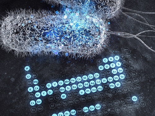
A KAIST bioprocess engineering research team led by Distinguished Professor Sang Yup Lee conducted a summary of 146 biosynthesized single and multi-element inorganic nanomaterials covering 55 elements in the periodic table synthesized using wild-type and genetically engineered microorganisms. Their research highlights the diverse applications of biogenic nanomaterials and gives strategies for improving the biosynthesis of nanomaterials in terms of their producibility, crystallinity, size, and shape.
The research team described a 10-step flow chart for developing the biosynthesis of inorganic nanomaterials using microorganisms and bacteriophages. The research was published at Nature Review Chemistry as a cover and hero paper on December 3.
“We suggest general strategies for microbial nanomaterial biosynthesis via a step-by-step flow chart and give our perspectives on the future of nanomaterial biosynthesis and applications. This flow chart will serve as a general guide for those wishing to prepare biosynthetic inorganic nanomaterials using microbial cells,” explained Dr.Yoojin Choi, a co-author of this research.
Most inorganic nanomaterials are produced using physical and chemical methods and biological synthesis has been gaining more and more attention. However, conventional synthesis processes have drawbacks in terms of high energy consumption and non-environmentally friendly processes. Meanwhile, microorganisms such as microalgae, yeasts, fungi, bacteria, and even viruses can be utilized as biofactories to produce single and multi-element inorganic nanomaterials under mild conditions.
After conducting a massive survey, the research team summed up that the development of genetically engineered microorganisms with increased inorganic-ion-binding affinity, inorganic-ion-reduction ability, and nanomaterial biosynthetic efficiency has enabled the synthesis of many inorganic nanomaterials.
Among the strategies, the team introduced their analysis of a Pourbaix diagram for controlling the size and morphology of a product. The research team said this Pourbaix diagram analysis can be widely employed for biosynthesizing new nanomaterials with industrial applications.Professor Sang Yup Lee added, “This research provides extensive information and perspectives on the biosynthesis of diverse inorganic nanomaterials using microorganisms and bacteriophages and their applications. We expect that biosynthetic inorganic nanomaterials will find more diverse and innovative applications across diverse fields of science and technology.”
Dr. Choi started this research in 2018 and her interview about completing this extensive research was featured in an article at Nature Career article on December 4.
-ProfileDistinguished Professor Sang Yup Lee leesy@kaist.ac.krMetabolic &Biomolecular Engineering National Research Laboratoryhttp://mbel.kaist.ac.krDepartment of Chemical and Biomolecular EngineeringKAIST
2020.12.07 View 12428
A Comprehensive Review of Biosynthesis of Inorganic Nanomaterials Using Microorganisms and Bacteriophages
There are diverse methods for producing numerous inorganic nanomaterials involving many experimental variables. Among the numerous possible matches, finding the best pair for synthesizing in an environmentally friendly way has been a longstanding challenge for researchers and industries.
A KAIST bioprocess engineering research team led by Distinguished Professor Sang Yup Lee conducted a summary of 146 biosynthesized single and multi-element inorganic nanomaterials covering 55 elements in the periodic table synthesized using wild-type and genetically engineered microorganisms. Their research highlights the diverse applications of biogenic nanomaterials and gives strategies for improving the biosynthesis of nanomaterials in terms of their producibility, crystallinity, size, and shape.
The research team described a 10-step flow chart for developing the biosynthesis of inorganic nanomaterials using microorganisms and bacteriophages. The research was published at Nature Review Chemistry as a cover and hero paper on December 3.
“We suggest general strategies for microbial nanomaterial biosynthesis via a step-by-step flow chart and give our perspectives on the future of nanomaterial biosynthesis and applications. This flow chart will serve as a general guide for those wishing to prepare biosynthetic inorganic nanomaterials using microbial cells,” explained Dr.Yoojin Choi, a co-author of this research.
Most inorganic nanomaterials are produced using physical and chemical methods and biological synthesis has been gaining more and more attention. However, conventional synthesis processes have drawbacks in terms of high energy consumption and non-environmentally friendly processes. Meanwhile, microorganisms such as microalgae, yeasts, fungi, bacteria, and even viruses can be utilized as biofactories to produce single and multi-element inorganic nanomaterials under mild conditions.
After conducting a massive survey, the research team summed up that the development of genetically engineered microorganisms with increased inorganic-ion-binding affinity, inorganic-ion-reduction ability, and nanomaterial biosynthetic efficiency has enabled the synthesis of many inorganic nanomaterials.
Among the strategies, the team introduced their analysis of a Pourbaix diagram for controlling the size and morphology of a product. The research team said this Pourbaix diagram analysis can be widely employed for biosynthesizing new nanomaterials with industrial applications.Professor Sang Yup Lee added, “This research provides extensive information and perspectives on the biosynthesis of diverse inorganic nanomaterials using microorganisms and bacteriophages and their applications. We expect that biosynthetic inorganic nanomaterials will find more diverse and innovative applications across diverse fields of science and technology.”
Dr. Choi started this research in 2018 and her interview about completing this extensive research was featured in an article at Nature Career article on December 4.
-ProfileDistinguished Professor Sang Yup Lee leesy@kaist.ac.krMetabolic &Biomolecular Engineering National Research Laboratoryhttp://mbel.kaist.ac.krDepartment of Chemical and Biomolecular EngineeringKAIST
2020.12.07 View 12428 -
 Scientist of October: Professor Jungwon Kim
Professor Jungwon Kim from the Department of Mechanical Engineering was selected as the ‘Scientist of the Month’ for October 2020 by the Ministry of Science and ICT and the National Research Foundation of Korea. Professor Kim was recognized for his contributions to expanding the horizons of the basics of precision engineering through his research on multifunctional ultrahigh-speed, high-resolution sensors. He received 10 million KRW in prize money.
Professor Kim was selected as the recipient of this award in celebration of “Measurement Day”, which commemorates October 26 as the day in which King Sejong the Great established a volume measurement system.
Professor Kim discovered that the time difference between the pulse of light created by a laser and the pulse of the current produced by a light-emitting diode was as small as 100 attoseconds (10-16 seconds). He then developed a unique multifunctional ultrahigh-speed, high-resolution Time-of-Flight (TOF) sensor that could take measurements of multiple points at the same time by sampling electric light. The sensor, with a measurement speed of 100 megahertz (100 million vibrations per second), a resolution of 180 picometers (1/5.5 billion meters), and a dynamic range of 150 decibels, overcame the limitations of both existing TOF techniques and laser interferometric techniques at the same time. The results of this research were published in Nature Photonics on February 10, 2020.
Professor Kim said, “I’d like to thank the graduate students who worked passionately with me, and KAIST for providing an environment in which I could fully focus on research. I am looking forward to the new and diverse applications in the field of machine manufacturing, such as studying the dynamic phenomena in microdevices, or taking ultraprecision measurement of shapes for advanced manufacturing.”
(END)
2020.10.15 View 13811
Scientist of October: Professor Jungwon Kim
Professor Jungwon Kim from the Department of Mechanical Engineering was selected as the ‘Scientist of the Month’ for October 2020 by the Ministry of Science and ICT and the National Research Foundation of Korea. Professor Kim was recognized for his contributions to expanding the horizons of the basics of precision engineering through his research on multifunctional ultrahigh-speed, high-resolution sensors. He received 10 million KRW in prize money.
Professor Kim was selected as the recipient of this award in celebration of “Measurement Day”, which commemorates October 26 as the day in which King Sejong the Great established a volume measurement system.
Professor Kim discovered that the time difference between the pulse of light created by a laser and the pulse of the current produced by a light-emitting diode was as small as 100 attoseconds (10-16 seconds). He then developed a unique multifunctional ultrahigh-speed, high-resolution Time-of-Flight (TOF) sensor that could take measurements of multiple points at the same time by sampling electric light. The sensor, with a measurement speed of 100 megahertz (100 million vibrations per second), a resolution of 180 picometers (1/5.5 billion meters), and a dynamic range of 150 decibels, overcame the limitations of both existing TOF techniques and laser interferometric techniques at the same time. The results of this research were published in Nature Photonics on February 10, 2020.
Professor Kim said, “I’d like to thank the graduate students who worked passionately with me, and KAIST for providing an environment in which I could fully focus on research. I am looking forward to the new and diverse applications in the field of machine manufacturing, such as studying the dynamic phenomena in microdevices, or taking ultraprecision measurement of shapes for advanced manufacturing.”
(END)
2020.10.15 View 13811 -
 Slippery When Wet: Fish and Seaweed Inspire Ships to Reduce Fluid Friction
Faster ships could be on the horizon after KAIST scientists develop a slippery surface inspired by fish and seaweed to reduce the hull's drag through the water.
Long-distance cargo ships lose a significant amount of energy due to fluid friction. Looking to the drag reduction mechanisms employed by aquatic life can provide inspiration on how to improve efficiency.
Fish and seaweed secrete a layer of mucus to create a slippery surface, reducing their friction as they travel through water. A potential way to mimic this is by creating lubricant-infused surfaces covered with cavities. As the cavities are continuously filled with the lubricant, a layer is formed over the surface.
Though this method has previously been shown to work, reducing drag by up to 18%, the underlying physics is not fully understood. KAIST researchers in collaboration with a team of researchers from POSTECH conducted simulations of this process to help explain the effects, and their findings were published in the journal Physics of Fluids on September 15.
The group looked at the average speed of a cargo ship with realistic material properties and simulated how it behaves under various lubrication setups. Specifically, they monitored the effects of the open area of the lubricant-filled cavities, as well as the thickness of the cavity lids.
They found that for larger open areas, the lubricant spreads more than it does with smaller open areas, leading to a slipperier surface. On the other hand, the lid thickness does not have much of an effect on the slip, though a thicker lid does create a thicker lubricant buildup layer.
Professor Emeritus Hyung Jin Sung from the KAIST Department of Mechanical Engineering who led this study said, “Our investigation of the hydrodynamics of a lubricant layer and how it results in drag reduction with a slippery surface in a basic configuration has provided significant insight into the benefits of a lubricant-infused surface.”
Now that they have worked on optimizing the lubricant secretion design, the authors hope it can be implemented in real-life marine vehicles.
“If the present design parameters are adopted, the drag reduction rate will increase significantly,” Professor Sung added.
This work was supported by the National Research Foundation (NRF) of Korea.
Source:
Materials provided by American Institute of Physics.
Publication:
Kim, Seung Joong, et al. (2020). A lubricant-infused slip surface for drag reduction. Physics of Fluids. Available online at https://doi.org/10.1063/5.0018460
Profile:
Hyung Jin Sung
Professor Emeritus
hyungjin@kaist.ac.kr
http://flow.kaist.ac.kr/index.php
Flow Control Lab. (FCL)
Department of Mechanical Engineering
http://kaist.ac.kr
Korea Advanced Institute of Science and Technology (KAIST)
Daejeon, Republic of Korea
(END)
2020.10.12 View 8512
Slippery When Wet: Fish and Seaweed Inspire Ships to Reduce Fluid Friction
Faster ships could be on the horizon after KAIST scientists develop a slippery surface inspired by fish and seaweed to reduce the hull's drag through the water.
Long-distance cargo ships lose a significant amount of energy due to fluid friction. Looking to the drag reduction mechanisms employed by aquatic life can provide inspiration on how to improve efficiency.
Fish and seaweed secrete a layer of mucus to create a slippery surface, reducing their friction as they travel through water. A potential way to mimic this is by creating lubricant-infused surfaces covered with cavities. As the cavities are continuously filled with the lubricant, a layer is formed over the surface.
Though this method has previously been shown to work, reducing drag by up to 18%, the underlying physics is not fully understood. KAIST researchers in collaboration with a team of researchers from POSTECH conducted simulations of this process to help explain the effects, and their findings were published in the journal Physics of Fluids on September 15.
The group looked at the average speed of a cargo ship with realistic material properties and simulated how it behaves under various lubrication setups. Specifically, they monitored the effects of the open area of the lubricant-filled cavities, as well as the thickness of the cavity lids.
They found that for larger open areas, the lubricant spreads more than it does with smaller open areas, leading to a slipperier surface. On the other hand, the lid thickness does not have much of an effect on the slip, though a thicker lid does create a thicker lubricant buildup layer.
Professor Emeritus Hyung Jin Sung from the KAIST Department of Mechanical Engineering who led this study said, “Our investigation of the hydrodynamics of a lubricant layer and how it results in drag reduction with a slippery surface in a basic configuration has provided significant insight into the benefits of a lubricant-infused surface.”
Now that they have worked on optimizing the lubricant secretion design, the authors hope it can be implemented in real-life marine vehicles.
“If the present design parameters are adopted, the drag reduction rate will increase significantly,” Professor Sung added.
This work was supported by the National Research Foundation (NRF) of Korea.
Source:
Materials provided by American Institute of Physics.
Publication:
Kim, Seung Joong, et al. (2020). A lubricant-infused slip surface for drag reduction. Physics of Fluids. Available online at https://doi.org/10.1063/5.0018460
Profile:
Hyung Jin Sung
Professor Emeritus
hyungjin@kaist.ac.kr
http://flow.kaist.ac.kr/index.php
Flow Control Lab. (FCL)
Department of Mechanical Engineering
http://kaist.ac.kr
Korea Advanced Institute of Science and Technology (KAIST)
Daejeon, Republic of Korea
(END)
2020.10.12 View 8512 -
 Deep Learning Helps Explore the Structural and Strategic Bases of Autism
Psychiatrists typically diagnose autism spectrum disorders (ASD) by observing a person’s behavior and by leaning on the Diagnostic and Statistical Manual of Mental Disorders (DSM-5), widely considered the “bible” of mental health diagnosis.
However, there are substantial differences amongst individuals on the spectrum and a great deal remains unknown by science about the causes of autism, or even what autism is. As a result, an accurate diagnosis of ASD and a prognosis prediction for patients can be extremely difficult.
But what if artificial intelligence (AI) could help? Deep learning, a type of AI, deploys artificial neural networks based on the human brain to recognize patterns in a way that is akin to, and in some cases can surpass, human ability. The technique, or rather suite of techniques, has enjoyed remarkable success in recent years in fields as diverse as voice recognition, translation, autonomous vehicles, and drug discovery.
A group of researchers from KAIST in collaboration with the Yonsei University College of Medicine has applied these deep learning techniques to autism diagnosis. Their findings were published on August 14 in the journal IEEE Access.
Magnetic resonance imaging (MRI) scans of brains of people known to have autism have been used by researchers and clinicians to try to identify structures of the brain they believed were associated with ASD. These researchers have achieved considerable success in identifying abnormal grey and white matter volume and irregularities in cerebral cortex activation and connections as being associated with the condition.
These findings have subsequently been deployed in studies attempting more consistent diagnoses of patients than has been achieved via psychiatrist observations during counseling sessions. While such studies have reported high levels of diagnostic accuracy, the number of participants in these studies has been small, often under 50, and diagnostic performance drops markedly when applied to large sample sizes or on datasets that include people from a wide variety of populations and locations.
“There was something as to what defines autism that human researchers and clinicians must have been overlooking,” said Keun-Ah Cheon, one of the two corresponding authors and a professor in Department of Child and Adolescent Psychiatry at Severance Hospital of the Yonsei University College of Medicine.
“And humans poring over thousands of MRI scans won’t be able to pick up on what we’ve been missing,” she continued. “But we thought AI might be able to.”
So the team applied five different categories of deep learning models to an open-source dataset of more than 1,000 MRI scans from the Autism Brain Imaging Data Exchange (ABIDE) initiative, which has collected brain imaging data from laboratories around the world, and to a smaller, but higher-resolution MRI image dataset (84 images) taken from the Child Psychiatric Clinic at Severance Hospital, Yonsei University College of Medicine. In both cases, the researchers used both structural MRIs (examining the anatomy of the brain) and functional MRIs (examining brain activity in different regions).
The models allowed the team to explore the structural bases of ASD brain region by brain region, focusing in particular on many structures below the cerebral cortex, including the basal ganglia, which are involved in motor function (movement) as well as learning and memory.
Crucially, these specific types of deep learning models also offered up possible explanations of how the AI had come up with its rationale for these findings.
“Understanding the way that the AI has classified these brain structures and dynamics is extremely important,” said Sang Wan Lee, the other corresponding author and an associate professor at KAIST. “It’s no good if a doctor can tell a patient that the computer says they have autism, but not be able to say why the computer knows that.”
The deep learning models were also able to describe how much a particular aspect contributed to ASD, an analysis tool that can assist psychiatric physicians during the diagnosis process to identify the severity of the autism.
“Doctors should be able to use this to offer a personalized diagnosis for patients, including a prognosis of how the condition could develop,” Lee said.
“Artificial intelligence is not going to put psychiatrists out of a job,” he explained. “But using AI as a tool should enable doctors to better understand and diagnose complex disorders than they could do on their own.”
-ProfileProfessor Sang Wan LeeDepartment of Bio and Brain EngineeringLaboratory for Brain and Machine Intelligence https://aibrain.kaist.ac.kr/
KAIST
2020.09.23 View 12561
Deep Learning Helps Explore the Structural and Strategic Bases of Autism
Psychiatrists typically diagnose autism spectrum disorders (ASD) by observing a person’s behavior and by leaning on the Diagnostic and Statistical Manual of Mental Disorders (DSM-5), widely considered the “bible” of mental health diagnosis.
However, there are substantial differences amongst individuals on the spectrum and a great deal remains unknown by science about the causes of autism, or even what autism is. As a result, an accurate diagnosis of ASD and a prognosis prediction for patients can be extremely difficult.
But what if artificial intelligence (AI) could help? Deep learning, a type of AI, deploys artificial neural networks based on the human brain to recognize patterns in a way that is akin to, and in some cases can surpass, human ability. The technique, or rather suite of techniques, has enjoyed remarkable success in recent years in fields as diverse as voice recognition, translation, autonomous vehicles, and drug discovery.
A group of researchers from KAIST in collaboration with the Yonsei University College of Medicine has applied these deep learning techniques to autism diagnosis. Their findings were published on August 14 in the journal IEEE Access.
Magnetic resonance imaging (MRI) scans of brains of people known to have autism have been used by researchers and clinicians to try to identify structures of the brain they believed were associated with ASD. These researchers have achieved considerable success in identifying abnormal grey and white matter volume and irregularities in cerebral cortex activation and connections as being associated with the condition.
These findings have subsequently been deployed in studies attempting more consistent diagnoses of patients than has been achieved via psychiatrist observations during counseling sessions. While such studies have reported high levels of diagnostic accuracy, the number of participants in these studies has been small, often under 50, and diagnostic performance drops markedly when applied to large sample sizes or on datasets that include people from a wide variety of populations and locations.
“There was something as to what defines autism that human researchers and clinicians must have been overlooking,” said Keun-Ah Cheon, one of the two corresponding authors and a professor in Department of Child and Adolescent Psychiatry at Severance Hospital of the Yonsei University College of Medicine.
“And humans poring over thousands of MRI scans won’t be able to pick up on what we’ve been missing,” she continued. “But we thought AI might be able to.”
So the team applied five different categories of deep learning models to an open-source dataset of more than 1,000 MRI scans from the Autism Brain Imaging Data Exchange (ABIDE) initiative, which has collected brain imaging data from laboratories around the world, and to a smaller, but higher-resolution MRI image dataset (84 images) taken from the Child Psychiatric Clinic at Severance Hospital, Yonsei University College of Medicine. In both cases, the researchers used both structural MRIs (examining the anatomy of the brain) and functional MRIs (examining brain activity in different regions).
The models allowed the team to explore the structural bases of ASD brain region by brain region, focusing in particular on many structures below the cerebral cortex, including the basal ganglia, which are involved in motor function (movement) as well as learning and memory.
Crucially, these specific types of deep learning models also offered up possible explanations of how the AI had come up with its rationale for these findings.
“Understanding the way that the AI has classified these brain structures and dynamics is extremely important,” said Sang Wan Lee, the other corresponding author and an associate professor at KAIST. “It’s no good if a doctor can tell a patient that the computer says they have autism, but not be able to say why the computer knows that.”
The deep learning models were also able to describe how much a particular aspect contributed to ASD, an analysis tool that can assist psychiatric physicians during the diagnosis process to identify the severity of the autism.
“Doctors should be able to use this to offer a personalized diagnosis for patients, including a prognosis of how the condition could develop,” Lee said.
“Artificial intelligence is not going to put psychiatrists out of a job,” he explained. “But using AI as a tool should enable doctors to better understand and diagnose complex disorders than they could do on their own.”
-ProfileProfessor Sang Wan LeeDepartment of Bio and Brain EngineeringLaboratory for Brain and Machine Intelligence https://aibrain.kaist.ac.kr/
KAIST
2020.09.23 View 12561 -
 Sturdy Fabric-Based Piezoelectric Energy Harvester Takes Us One Step Closer to Wearable Electronics
KAIST researchers presented a highly flexible but sturdy wearable piezoelectric harvester using the simple and easy fabrication process of hot pressing and tape casting. This energy harvester, which has record high interfacial adhesion strength, will take us one step closer to being able to manufacture embedded wearable electronics.
A research team led by Professor Seungbum Hong said that the novelty of this result lies in its simplicity, applicability, durability, and its new characterization of wearable electronic devices.
Wearable devices are increasingly being used in a wide array of applications from small electronics to embedded devices such as sensors, actuators, displays, and energy harvesters.
Despite their many advantages, high costs and complex fabrication processes remained challenges for reaching commercialization. In addition, their durability was frequently questioned. To address these issues, Professor Hong’s team developed a new fabrication process and analysis technology for testing the mechanical properties of affordable wearable devices.
For this process, the research team used a hot pressing and tape casting procedure to connect the fabric structures of polyester and a polymer film. Hot pressing has usually been used when making batteries and fuel cells due to its high adhesiveness. Above all, the process takes only two to three minutes.
The newly developed fabrication process will enable the direct application of a device into general garments using hot pressing just as graphic patches can be attached to garments using a heat press.
In particular, when the polymer film is hot pressed onto a fabric below its crystallization temperature, it transforms into an amorphous state. In this state, it compactly attaches to the concave surface of the fabric and infiltrates into the gaps between the transverse wefts and longitudinal warps. These features result in high interfacial adhesion strength. For this reason, hot pressing has the potential to reduce the cost of fabrication through the direct application of fabric-based wearable devices to common garments.
In addition to the conventional durability test of bending cycles, the newly introduced surface and interfacial cutting analysis system proved the high mechanical durability of the fabric-based wearable device by measuring the high interfacial adhesion strength between the fabric and the polymer film. Professor Hong said the study lays a new foundation for the manufacturing process and analysis of wearable devices using fabrics and polymers.
He added that his team first used the surface and interfacial cutting analysis system (SAICAS) in the field of wearable electronics to test the mechanical properties of polymer-based wearable devices. Their surface and interfacial cutting analysis system is more precise than conventional methods (peel test, tape test, and microstretch test) because it qualitatively and quantitatively measures the adhesion strength.
Professor Hong explained, “This study could enable the commercialization of highly durable wearable devices based on the analysis of their interfacial adhesion strength. Our study lays a new foundation for the manufacturing process and analysis of other devices using fabrics and polymers. We look forward to fabric-based wearable electronics hitting the market very soon.”
The results of this study were registered as a domestic patent in Korea last year, and published in Nano Energy this month. This study has been conducted through collaboration with Professor Yong Min Lee in the Department of Energy Science and Engineering at DGIST, Professor Kwangsoo No in the Department of Materials Science and Engineering at KAIST, and Professor Seunghwa Ryu in the Department of Mechanical Engineering at KAIST.
This study was supported by the High-Risk High-Return Project and the Global Singularity Research Project at KAIST, the National Research Foundation, and the Ministry of Science and ICT in Korea.
-Publication:
Jaegyu Kim, Seoungwoo Byun, Sangryun Lee, Jeongjae Ryu, Seongwoo Cho, Chungik Oh, Hongjun Kim, Kwangsoo No, Seunghwa Ryu, Yong Min Lee, Seungbum Hong*, Nano Energy 75 (2020), 104992.
https://doi.org/10.1016/j.nanoen.2020.104992
-Profile: Professor Seungbum Hong
seungbum@kaist.ac.kr
http://mii.kaist.ac.kr/
Department of Materials Science and Engineering
KAIST
2020.09.17 View 15114
Sturdy Fabric-Based Piezoelectric Energy Harvester Takes Us One Step Closer to Wearable Electronics
KAIST researchers presented a highly flexible but sturdy wearable piezoelectric harvester using the simple and easy fabrication process of hot pressing and tape casting. This energy harvester, which has record high interfacial adhesion strength, will take us one step closer to being able to manufacture embedded wearable electronics.
A research team led by Professor Seungbum Hong said that the novelty of this result lies in its simplicity, applicability, durability, and its new characterization of wearable electronic devices.
Wearable devices are increasingly being used in a wide array of applications from small electronics to embedded devices such as sensors, actuators, displays, and energy harvesters.
Despite their many advantages, high costs and complex fabrication processes remained challenges for reaching commercialization. In addition, their durability was frequently questioned. To address these issues, Professor Hong’s team developed a new fabrication process and analysis technology for testing the mechanical properties of affordable wearable devices.
For this process, the research team used a hot pressing and tape casting procedure to connect the fabric structures of polyester and a polymer film. Hot pressing has usually been used when making batteries and fuel cells due to its high adhesiveness. Above all, the process takes only two to three minutes.
The newly developed fabrication process will enable the direct application of a device into general garments using hot pressing just as graphic patches can be attached to garments using a heat press.
In particular, when the polymer film is hot pressed onto a fabric below its crystallization temperature, it transforms into an amorphous state. In this state, it compactly attaches to the concave surface of the fabric and infiltrates into the gaps between the transverse wefts and longitudinal warps. These features result in high interfacial adhesion strength. For this reason, hot pressing has the potential to reduce the cost of fabrication through the direct application of fabric-based wearable devices to common garments.
In addition to the conventional durability test of bending cycles, the newly introduced surface and interfacial cutting analysis system proved the high mechanical durability of the fabric-based wearable device by measuring the high interfacial adhesion strength between the fabric and the polymer film. Professor Hong said the study lays a new foundation for the manufacturing process and analysis of wearable devices using fabrics and polymers.
He added that his team first used the surface and interfacial cutting analysis system (SAICAS) in the field of wearable electronics to test the mechanical properties of polymer-based wearable devices. Their surface and interfacial cutting analysis system is more precise than conventional methods (peel test, tape test, and microstretch test) because it qualitatively and quantitatively measures the adhesion strength.
Professor Hong explained, “This study could enable the commercialization of highly durable wearable devices based on the analysis of their interfacial adhesion strength. Our study lays a new foundation for the manufacturing process and analysis of other devices using fabrics and polymers. We look forward to fabric-based wearable electronics hitting the market very soon.”
The results of this study were registered as a domestic patent in Korea last year, and published in Nano Energy this month. This study has been conducted through collaboration with Professor Yong Min Lee in the Department of Energy Science and Engineering at DGIST, Professor Kwangsoo No in the Department of Materials Science and Engineering at KAIST, and Professor Seunghwa Ryu in the Department of Mechanical Engineering at KAIST.
This study was supported by the High-Risk High-Return Project and the Global Singularity Research Project at KAIST, the National Research Foundation, and the Ministry of Science and ICT in Korea.
-Publication:
Jaegyu Kim, Seoungwoo Byun, Sangryun Lee, Jeongjae Ryu, Seongwoo Cho, Chungik Oh, Hongjun Kim, Kwangsoo No, Seunghwa Ryu, Yong Min Lee, Seungbum Hong*, Nano Energy 75 (2020), 104992.
https://doi.org/10.1016/j.nanoen.2020.104992
-Profile: Professor Seungbum Hong
seungbum@kaist.ac.kr
http://mii.kaist.ac.kr/
Department of Materials Science and Engineering
KAIST
2020.09.17 View 15114 -
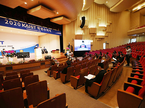 Virtual Commencement Ceremony Honors the Class of 2020
The KAIST community gathered online to celebrate the 2020 graduating class. The blended ceremony conferred their hard-earned degrees on August 28. The belated celebration, which was postponed from February 21 due to the COVID-19 outbreak, honored the 2846 graduates with live streaming on YouTube beginning at 2:00 pm. The graduates include 721 PhDs and 1399 master’s degree holders.
The government raised its social distancing guidelines to level two out of three on August 23 as the second wave of the virus hit the nation. Level two guidelines prohibit the gathering of more than 50 persons indoors or 100 persons outdoors.
For the virtual ceremony, the Office of Student Affairs and Policy announced a list of 67 graduates who signed up to participate in the graduation ceremony. Graduates were divided into three groups to attend at three different places and watch the ceremony via Zoom. No family and friends of the graduates were allowed to participate at the campus.
This year’s valedictorian, Kon-Yong Lee from the Department of Chemical and Biomolecular Engineering, received the Award of Minister of Science and Technology. Salutorian Hee-Kwang Roh from the Department of Chemistry received the Award of the KAIST Board of Trustees, while the recipient of the KAIST Presidential Award was Hong Jae-Min from the School of Computing.
President Sung-Chul Shin, Chairman of the Board of Trustees Woo-Sik Kim, former Minister of Science and Technology and former Provost at KAIST Dr. KunMo Chung, and a very limited number of faculty and staff members officiated the commencement ceremony from the KAIST auditorium.
President Shin in his commencement speech applauded the graduates’ hard work and dedication and delivered a very special congratulatory message to them. He encouraged the new graduates to be courageous enough to deal with these new challenges as well as future uncertainties, during the greatest transformation brought about by COVID-19.
“Instead of following behind others as a fast follower, we should take the initiative and walk down new paths as a first mover.” He also stressed, “We can transform this crisis into an opportunity by practicing the C3 values KAIST pursues: Challenging, Creating, and Caring.”
As new alumni of Korea’s top science and technology university, he said, “Our graduates should focus on creating the world’s best, first, or only one in their research or their work.” However, he also pointed out the importance of a caring mind for others when working together.
At the ceremony, KAIST conferred an honorary doctorate degree to Dr. Younghoon David Kim, CEO and Chairman of Daesung Group, in recognition of his lifetime dedication to making innovations in the energy industry.
Daesung Group is a leading energy company in Korea which manufactures and supplies natural gas for industries and home users. Dr. Kim is committed to making efficient energy sources by advancing cutting-energy sciences and disruptive technologies. He has served as chairman of the World Energy Council since 2016.
In his acceptance speech, Kim stressed the Grand Energy Transition as a new driving force in the future energy industry for maximizing energy efficiency.
“Since energy is the most basic foundation for all industries, improvements in energy efficiency translate into benefits for all related industries in terms of its efficiency and productivity.”
“The Grand Energy Transition is progressing widely and rapidly across the entire value chain of energy production, distribution, and consumption with decarbonization, decentralization, and digitalization serving as its driving force.”
He went on, “We should regard energy efficiency not as the fifth fuel but the first primary fuel.”
(END)
2020.08.28 View 13032
Virtual Commencement Ceremony Honors the Class of 2020
The KAIST community gathered online to celebrate the 2020 graduating class. The blended ceremony conferred their hard-earned degrees on August 28. The belated celebration, which was postponed from February 21 due to the COVID-19 outbreak, honored the 2846 graduates with live streaming on YouTube beginning at 2:00 pm. The graduates include 721 PhDs and 1399 master’s degree holders.
The government raised its social distancing guidelines to level two out of three on August 23 as the second wave of the virus hit the nation. Level two guidelines prohibit the gathering of more than 50 persons indoors or 100 persons outdoors.
For the virtual ceremony, the Office of Student Affairs and Policy announced a list of 67 graduates who signed up to participate in the graduation ceremony. Graduates were divided into three groups to attend at three different places and watch the ceremony via Zoom. No family and friends of the graduates were allowed to participate at the campus.
This year’s valedictorian, Kon-Yong Lee from the Department of Chemical and Biomolecular Engineering, received the Award of Minister of Science and Technology. Salutorian Hee-Kwang Roh from the Department of Chemistry received the Award of the KAIST Board of Trustees, while the recipient of the KAIST Presidential Award was Hong Jae-Min from the School of Computing.
President Sung-Chul Shin, Chairman of the Board of Trustees Woo-Sik Kim, former Minister of Science and Technology and former Provost at KAIST Dr. KunMo Chung, and a very limited number of faculty and staff members officiated the commencement ceremony from the KAIST auditorium.
President Shin in his commencement speech applauded the graduates’ hard work and dedication and delivered a very special congratulatory message to them. He encouraged the new graduates to be courageous enough to deal with these new challenges as well as future uncertainties, during the greatest transformation brought about by COVID-19.
“Instead of following behind others as a fast follower, we should take the initiative and walk down new paths as a first mover.” He also stressed, “We can transform this crisis into an opportunity by practicing the C3 values KAIST pursues: Challenging, Creating, and Caring.”
As new alumni of Korea’s top science and technology university, he said, “Our graduates should focus on creating the world’s best, first, or only one in their research or their work.” However, he also pointed out the importance of a caring mind for others when working together.
At the ceremony, KAIST conferred an honorary doctorate degree to Dr. Younghoon David Kim, CEO and Chairman of Daesung Group, in recognition of his lifetime dedication to making innovations in the energy industry.
Daesung Group is a leading energy company in Korea which manufactures and supplies natural gas for industries and home users. Dr. Kim is committed to making efficient energy sources by advancing cutting-energy sciences and disruptive technologies. He has served as chairman of the World Energy Council since 2016.
In his acceptance speech, Kim stressed the Grand Energy Transition as a new driving force in the future energy industry for maximizing energy efficiency.
“Since energy is the most basic foundation for all industries, improvements in energy efficiency translate into benefits for all related industries in terms of its efficiency and productivity.”
“The Grand Energy Transition is progressing widely and rapidly across the entire value chain of energy production, distribution, and consumption with decarbonization, decentralization, and digitalization serving as its driving force.”
He went on, “We should regard energy efficiency not as the fifth fuel but the first primary fuel.”
(END)
2020.08.28 View 13032 -
 Before Eyes Open, They Get Ready to See
- Spontaneous retinal waves can generate long-range horizontal connectivity in visual cortex. -
A KAIST research team’s computational simulations demonstrated that the waves of spontaneous neural activity in the retinas of still-closed eyes in mammals develop long-range horizontal connections in the visual cortex during early developmental stages.
This new finding featured in the August 19 edition of Journal of Neuroscience as a cover article has resolved a long-standing puzzle for understanding visual neuroscience regarding the early organization of functional architectures in the mammalian visual cortex before eye-opening, especially the long-range horizontal connectivity known as “feature-specific” circuitry.
To prepare the animal to see when its eyes open, neural circuits in the brain’s visual system must begin developing earlier. However, the proper development of many brain regions involved in vision generally requires sensory input through the eyes.
In the primary visual cortex of the higher mammalian taxa, cortical neurons of similar functional tuning to a visual feature are linked together by long-range horizontal circuits that play a crucial role in visual information processing.
Surprisingly, these long-range horizontal connections in the primary visual cortex of higher mammals emerge before the onset of sensory experience, and the mechanism underlying this phenomenon has remained elusive.
To investigate this mechanism, a group of researchers led by Professor Se-Bum Paik from the Department of Bio and Brain Engineering at KAIST implemented computational simulations of early visual pathways using data obtained from the retinal circuits in young animals before eye-opening, including cats, monkeys, and mice.
From these simulations, the researchers found that spontaneous waves propagating in ON and OFF retinal mosaics can initialize the wiring of long-range horizontal connections by selectively co-activating cortical neurons of similar functional tuning, whereas equivalent random activities cannot induce such organizations.
The simulations also showed that emerged long-range horizontal connections can induce the patterned cortical activities, matching the topography of underlying functional maps even in salt-and-pepper type organizations observed in rodents. This result implies that the model developed by Professor Paik and his group can provide a universal principle for the developmental mechanism of long-range horizontal connections in both higher mammals as well as rodents.
Professor Paik said, “Our model provides a deeper understanding of how the functional architectures in the visual cortex can originate from the spatial organization of the periphery, without sensory experience during early developmental periods.”
He continued, “We believe that our findings will be of great interest to scientists working in a wide range of fields such as neuroscience, vision science, and developmental biology.”
This work was supported by the National Research Foundation of Korea (NRF). Undergraduate student Jinwoo Kim participated in this research project and presented the findings as the lead author as part of the Undergraduate Research Participation (URP) Program at KAIST.
Figures and image credit: Professor Se-Bum Paik, KAIST
Image usage restrictions: News organizations may use or redistribute these figures and image, with proper attribution, as part of news coverage of this paper only.
Publication:
Jinwoo Kim, Min Song, and Se-Bum Paik. (2020). Spontaneous retinal waves generate long-range horizontal connectivity in visual cortex. Journal of Neuroscience, Available online athttps://www.jneurosci.org/content/early/2020/07/17/JNEUROSCI.0649-20.2020
Profile: Se-Bum Paik
Assistant Professor
sbpaik@kaist.ac.kr
http://vs.kaist.ac.kr/
VSNN Laboratory
Department of Bio and Brain Engineering
Program of Brain and Cognitive Engineering
http://kaist.ac.kr
Korea Advanced Institute of Science and Technology (KAIST) Daejeon, Republic of Korea
Profile: Jinwoo Kim
Undergraduate Student
bugkjw@kaist.ac.kr
Department of Bio and Brain Engineering, KAIST
Profile: Min Song
Ph.D. Candidate
night@kaist.ac.kr
Program of Brain and Cognitive Engineering, KAIST
(END)
2020.08.25 View 14757
Before Eyes Open, They Get Ready to See
- Spontaneous retinal waves can generate long-range horizontal connectivity in visual cortex. -
A KAIST research team’s computational simulations demonstrated that the waves of spontaneous neural activity in the retinas of still-closed eyes in mammals develop long-range horizontal connections in the visual cortex during early developmental stages.
This new finding featured in the August 19 edition of Journal of Neuroscience as a cover article has resolved a long-standing puzzle for understanding visual neuroscience regarding the early organization of functional architectures in the mammalian visual cortex before eye-opening, especially the long-range horizontal connectivity known as “feature-specific” circuitry.
To prepare the animal to see when its eyes open, neural circuits in the brain’s visual system must begin developing earlier. However, the proper development of many brain regions involved in vision generally requires sensory input through the eyes.
In the primary visual cortex of the higher mammalian taxa, cortical neurons of similar functional tuning to a visual feature are linked together by long-range horizontal circuits that play a crucial role in visual information processing.
Surprisingly, these long-range horizontal connections in the primary visual cortex of higher mammals emerge before the onset of sensory experience, and the mechanism underlying this phenomenon has remained elusive.
To investigate this mechanism, a group of researchers led by Professor Se-Bum Paik from the Department of Bio and Brain Engineering at KAIST implemented computational simulations of early visual pathways using data obtained from the retinal circuits in young animals before eye-opening, including cats, monkeys, and mice.
From these simulations, the researchers found that spontaneous waves propagating in ON and OFF retinal mosaics can initialize the wiring of long-range horizontal connections by selectively co-activating cortical neurons of similar functional tuning, whereas equivalent random activities cannot induce such organizations.
The simulations also showed that emerged long-range horizontal connections can induce the patterned cortical activities, matching the topography of underlying functional maps even in salt-and-pepper type organizations observed in rodents. This result implies that the model developed by Professor Paik and his group can provide a universal principle for the developmental mechanism of long-range horizontal connections in both higher mammals as well as rodents.
Professor Paik said, “Our model provides a deeper understanding of how the functional architectures in the visual cortex can originate from the spatial organization of the periphery, without sensory experience during early developmental periods.”
He continued, “We believe that our findings will be of great interest to scientists working in a wide range of fields such as neuroscience, vision science, and developmental biology.”
This work was supported by the National Research Foundation of Korea (NRF). Undergraduate student Jinwoo Kim participated in this research project and presented the findings as the lead author as part of the Undergraduate Research Participation (URP) Program at KAIST.
Figures and image credit: Professor Se-Bum Paik, KAIST
Image usage restrictions: News organizations may use or redistribute these figures and image, with proper attribution, as part of news coverage of this paper only.
Publication:
Jinwoo Kim, Min Song, and Se-Bum Paik. (2020). Spontaneous retinal waves generate long-range horizontal connectivity in visual cortex. Journal of Neuroscience, Available online athttps://www.jneurosci.org/content/early/2020/07/17/JNEUROSCI.0649-20.2020
Profile: Se-Bum Paik
Assistant Professor
sbpaik@kaist.ac.kr
http://vs.kaist.ac.kr/
VSNN Laboratory
Department of Bio and Brain Engineering
Program of Brain and Cognitive Engineering
http://kaist.ac.kr
Korea Advanced Institute of Science and Technology (KAIST) Daejeon, Republic of Korea
Profile: Jinwoo Kim
Undergraduate Student
bugkjw@kaist.ac.kr
Department of Bio and Brain Engineering, KAIST
Profile: Min Song
Ph.D. Candidate
night@kaist.ac.kr
Program of Brain and Cognitive Engineering, KAIST
(END)
2020.08.25 View 14757 -
 Professor Jaehyouk Choi, IT Young Engineer of the Year
Professor Jaehyouk Choi from the KAIST School of Electrical Engineering won the ‘IT Young Engineer Award’ for 2020. The award was co-presented by the Institute of Electrical and Electronics Engineers (IEEE) and the Institute of Electronics Engineers of Korea (IEIE), and sponsored by the Haedong Science and Culture Foundation.
The ‘IT Young Engineer Award’ selects only one mid-career scientist or engineer 40 years old or younger every year, who has made a great contribution to academic or technological advancements in the field of IT.
Professor Choi’s research topics include high-performance semiconductor circuit design for ultrahigh-speed communication systems including 5G communication. In particular, he is widely known for his field of the ‘ultra-low-noise, high-frequency signal generation circuit,’ key technology for next-generation wired and wireless communications, as well as for memory systems. He has published 64 papers in SCI journals and at international conferences, and applied for and registered 25 domestic and international patents.
Professor Choi is also an active member of the Technical Program Committee of international symposiums in the field of semiconductor circuits including the International Solid-State Circuits Conference (ISSCC) and the European Solid-State Circuit Conference (ESSCIRC). Beginning this year, he also serves as a distinguished lecturer at the IEEE Solid-State Circuit Society (SSCS).
(END)
2020.08.20 View 12662
Professor Jaehyouk Choi, IT Young Engineer of the Year
Professor Jaehyouk Choi from the KAIST School of Electrical Engineering won the ‘IT Young Engineer Award’ for 2020. The award was co-presented by the Institute of Electrical and Electronics Engineers (IEEE) and the Institute of Electronics Engineers of Korea (IEIE), and sponsored by the Haedong Science and Culture Foundation.
The ‘IT Young Engineer Award’ selects only one mid-career scientist or engineer 40 years old or younger every year, who has made a great contribution to academic or technological advancements in the field of IT.
Professor Choi’s research topics include high-performance semiconductor circuit design for ultrahigh-speed communication systems including 5G communication. In particular, he is widely known for his field of the ‘ultra-low-noise, high-frequency signal generation circuit,’ key technology for next-generation wired and wireless communications, as well as for memory systems. He has published 64 papers in SCI journals and at international conferences, and applied for and registered 25 domestic and international patents.
Professor Choi is also an active member of the Technical Program Committee of international symposiums in the field of semiconductor circuits including the International Solid-State Circuits Conference (ISSCC) and the European Solid-State Circuit Conference (ESSCIRC). Beginning this year, he also serves as a distinguished lecturer at the IEEE Solid-State Circuit Society (SSCS).
(END)
2020.08.20 View 12662 -
 KAIST Technology Value Tops in Commercialization Market
KAIST became the first Korean university to achieve 10.183 billion KRW in annual technology royalties, and was also selected as an ‘Institution of Outstanding Patent Quality Management’ and an ‘Institution of Outstanding Public Patent Technology Transfer’ for 2020.
KAIST earns its technology royalties through 56 technology transfer contracts. Following KAIST in the rankings were Seoul National University (SNU) in second place with 8.8 billion KRW from 87 contracts and Korea University (KU) in the third with 5.4 billion KRW from 133 contracts. The data shows the high value of KAIST-created technology in the market.
The Korean Intellectual Property Office (KIPO) started to recognize the Institution of Outstanding Patent Quality Management this year to encourage profit-driven patent management at universities and public research institutes, and KAIST was selected as one of the four first recipients of this distinction.
In addition, KAIST was selected as an Institution of Outstanding Public Patent Technology Transfer, a title given by KIPO to three universities and public research institutes this year with outstanding achievements in technology transfers and commercialization to encourage patent utilization.
Director of the KAIST Institute of Technology Value Creation (ITVC) Professor Kyung-cheol Choi said that KAIST’s achievement in annual technology royalties and technology transfers and commercialization were prime examples of accelerating competitiveness in intellectual property through innovative R&D investment.
In April, KAIST expanded and reorganized its Industry-Academia Collaboration Team into the ITVC to support technology transfers and commercialization. Specialized organizations such as the Intellectual Property and Technology Transfer Center and Industrial Liaison Center have been established under the ITVC, and industry experts have been recruited as special professors focusing on industry-academia collaborations to enhance its specialized functions.
KAIST also operates an enterprise membership system and technology consulting system, aimed at sharing its outstanding intellectual property within domestic industries. In 2019, it secured a technology transfer commercialization fund of 1.2 billion KRW available for three years under KIPO’s Intellectual Property Profit Reinvestment Support Program (formerly the Korean Patent Gap Fund Creation Project).
This program was introduced to bridge the gap between the technology developed in universities and the level of technology required by industry. Under the program, bold investments are made in early-stage technologies at the research paper or experiment phase.
The program encourages enterprises to take active steps for the transfer of technologies by demonstrating their commercial potential through prototype production, testing and certification, and standard patent filing. KAIST is currently funding approximately 20 new technologies under this program as of July 2020.
KAIST’s outstanding intellectual property management has also received international recognition, with its selection as Asia’s leading institution in university R&D intellectual property at the Intellectual Property Business Congress (IPBC) Asia 2019 held in Tokyo, Japan last October.
(END)
2020.08.18 View 11862
KAIST Technology Value Tops in Commercialization Market
KAIST became the first Korean university to achieve 10.183 billion KRW in annual technology royalties, and was also selected as an ‘Institution of Outstanding Patent Quality Management’ and an ‘Institution of Outstanding Public Patent Technology Transfer’ for 2020.
KAIST earns its technology royalties through 56 technology transfer contracts. Following KAIST in the rankings were Seoul National University (SNU) in second place with 8.8 billion KRW from 87 contracts and Korea University (KU) in the third with 5.4 billion KRW from 133 contracts. The data shows the high value of KAIST-created technology in the market.
The Korean Intellectual Property Office (KIPO) started to recognize the Institution of Outstanding Patent Quality Management this year to encourage profit-driven patent management at universities and public research institutes, and KAIST was selected as one of the four first recipients of this distinction.
In addition, KAIST was selected as an Institution of Outstanding Public Patent Technology Transfer, a title given by KIPO to three universities and public research institutes this year with outstanding achievements in technology transfers and commercialization to encourage patent utilization.
Director of the KAIST Institute of Technology Value Creation (ITVC) Professor Kyung-cheol Choi said that KAIST’s achievement in annual technology royalties and technology transfers and commercialization were prime examples of accelerating competitiveness in intellectual property through innovative R&D investment.
In April, KAIST expanded and reorganized its Industry-Academia Collaboration Team into the ITVC to support technology transfers and commercialization. Specialized organizations such as the Intellectual Property and Technology Transfer Center and Industrial Liaison Center have been established under the ITVC, and industry experts have been recruited as special professors focusing on industry-academia collaborations to enhance its specialized functions.
KAIST also operates an enterprise membership system and technology consulting system, aimed at sharing its outstanding intellectual property within domestic industries. In 2019, it secured a technology transfer commercialization fund of 1.2 billion KRW available for three years under KIPO’s Intellectual Property Profit Reinvestment Support Program (formerly the Korean Patent Gap Fund Creation Project).
This program was introduced to bridge the gap between the technology developed in universities and the level of technology required by industry. Under the program, bold investments are made in early-stage technologies at the research paper or experiment phase.
The program encourages enterprises to take active steps for the transfer of technologies by demonstrating their commercial potential through prototype production, testing and certification, and standard patent filing. KAIST is currently funding approximately 20 new technologies under this program as of July 2020.
KAIST’s outstanding intellectual property management has also received international recognition, with its selection as Asia’s leading institution in university R&D intellectual property at the Intellectual Property Business Congress (IPBC) Asia 2019 held in Tokyo, Japan last October.
(END)
2020.08.18 View 11862 -
 Deep Learning-Based Cough Recognition Model Helps Detect the Location of Coughing Sounds in Real Time
The Center for Noise and Vibration Control at KAIST announced that their coughing detection camera recognizes where coughing happens, visualizing the locations. The resulting cough recognition camera can track and record information about the person who coughed, their location, and the number of coughs on a real-time basis.
Professor Yong-Hwa Park from the Department of Mechanical Engineering developed a deep learning-based cough recognition model to classify a coughing sound in real time. The coughing event classification model is combined with a sound camera that visualizes their locations in public places. The research team said they achieved a best test accuracy of 87.4 %.
Professor Park said that it will be useful medical equipment during epidemics in public places such as schools, offices, and restaurants, and to constantly monitor patients’ conditions in a hospital room.
Fever and coughing are the most relevant respiratory disease symptoms, among which fever can be recognized remotely using thermal cameras. This new technology is expected to be very helpful for detecting epidemic transmissions in a non-contact way. The cough event classification model is combined with a sound camera that visualizes the cough event and indicates the location in the video image.
To develop a cough recognition model, a supervised learning was conducted with a convolutional neural network (CNN). The model performs binary classification with an input of a one-second sound profile feature, generating output to be either a cough event or something else.
In the training and evaluation, various datasets were collected from Audioset, DEMAND, ETSI, and TIMIT. Coughing and others sounds were extracted from Audioset, and the rest of the datasets were used as background noises for data augmentation so that this model could be generalized for various background noises in public places.
The dataset was augmented by mixing coughing sounds and other sounds from Audioset and background noises with the ratio of 0.15 to 0.75, then the overall volume was adjusted to 0.25 to 1.0 times to generalize the model for various distances.
The training and evaluation datasets were constructed by dividing the augmented dataset by 9:1, and the test dataset was recorded separately in a real office environment.
In the optimization procedure of the network model, training was conducted with various combinations of five acoustic features including spectrogram, Mel-scaled spectrogram and Mel-frequency cepstrum coefficients with seven optimizers. The performance of each combination was compared with the test dataset. The best test accuracy of 87.4% was achieved with Mel-scaled Spectrogram as the acoustic feature and ASGD as the optimizer.
The trained cough recognition model was combined with a sound camera. The sound camera is composed of a microphone array and a camera module. A beamforming process is applied to a collected set of acoustic data to find out the direction of incoming sound source. The integrated cough recognition model determines whether the sound is cough or not. If it is, the location of cough is visualized as a contour image with a ‘cough’ label at the location of the coughing sound source in a video image.
A pilot test of the cough recognition camera in an office environment shows that it successfully distinguishes cough events and other events even in a noisy environment. In addition, it can track the location of the person who coughed and count the number of coughs in real time. The performance will be improved further with additional training data obtained from other real environments such as hospitals and classrooms.
Professor Park said, “In a pandemic situation like we are experiencing with COVID-19, a cough detection camera can contribute to the prevention and early detection of epidemics in public places. Especially when applied to a hospital room, the patient's condition can be tracked 24 hours a day and support more accurate diagnoses while reducing the effort of the medical staff."
This study was conducted in collaboration with SM Instruments Inc.
Profile: Yong-Hwa Park, Ph.D.
Associate Professor
yhpark@kaist.ac.kr
http://human.kaist.ac.kr/
Human-Machine Interaction Laboratory (HuMaN Lab.)
Department of Mechanical Engineering (ME)
Korea Advanced Institute of Science and Technology (KAIST)
https://www.kaist.ac.kr/en/
Daejeon 34141, Korea
Profile: Gyeong Tae Lee
PhD Candidate
hansaram@kaist.ac.kr
HuMaN Lab., ME, KAIST
Profile: Seong Hu Kim
PhD Candidate
tjdgnkim@kaist.ac.kr
HuMaN Lab., ME, KAIST
Profile: Hyeonuk Nam
PhD Candidate
frednam@kaist.ac.kr
HuMaN Lab., ME, KAIST
Profile: Young-Key Kim
CEO
sales@smins.co.kr
http://en.smins.co.kr/
SM Instruments Inc.
Daejeon 34109, Korea
(END)
2020.08.13 View 18398
Deep Learning-Based Cough Recognition Model Helps Detect the Location of Coughing Sounds in Real Time
The Center for Noise and Vibration Control at KAIST announced that their coughing detection camera recognizes where coughing happens, visualizing the locations. The resulting cough recognition camera can track and record information about the person who coughed, their location, and the number of coughs on a real-time basis.
Professor Yong-Hwa Park from the Department of Mechanical Engineering developed a deep learning-based cough recognition model to classify a coughing sound in real time. The coughing event classification model is combined with a sound camera that visualizes their locations in public places. The research team said they achieved a best test accuracy of 87.4 %.
Professor Park said that it will be useful medical equipment during epidemics in public places such as schools, offices, and restaurants, and to constantly monitor patients’ conditions in a hospital room.
Fever and coughing are the most relevant respiratory disease symptoms, among which fever can be recognized remotely using thermal cameras. This new technology is expected to be very helpful for detecting epidemic transmissions in a non-contact way. The cough event classification model is combined with a sound camera that visualizes the cough event and indicates the location in the video image.
To develop a cough recognition model, a supervised learning was conducted with a convolutional neural network (CNN). The model performs binary classification with an input of a one-second sound profile feature, generating output to be either a cough event or something else.
In the training and evaluation, various datasets were collected from Audioset, DEMAND, ETSI, and TIMIT. Coughing and others sounds were extracted from Audioset, and the rest of the datasets were used as background noises for data augmentation so that this model could be generalized for various background noises in public places.
The dataset was augmented by mixing coughing sounds and other sounds from Audioset and background noises with the ratio of 0.15 to 0.75, then the overall volume was adjusted to 0.25 to 1.0 times to generalize the model for various distances.
The training and evaluation datasets were constructed by dividing the augmented dataset by 9:1, and the test dataset was recorded separately in a real office environment.
In the optimization procedure of the network model, training was conducted with various combinations of five acoustic features including spectrogram, Mel-scaled spectrogram and Mel-frequency cepstrum coefficients with seven optimizers. The performance of each combination was compared with the test dataset. The best test accuracy of 87.4% was achieved with Mel-scaled Spectrogram as the acoustic feature and ASGD as the optimizer.
The trained cough recognition model was combined with a sound camera. The sound camera is composed of a microphone array and a camera module. A beamforming process is applied to a collected set of acoustic data to find out the direction of incoming sound source. The integrated cough recognition model determines whether the sound is cough or not. If it is, the location of cough is visualized as a contour image with a ‘cough’ label at the location of the coughing sound source in a video image.
A pilot test of the cough recognition camera in an office environment shows that it successfully distinguishes cough events and other events even in a noisy environment. In addition, it can track the location of the person who coughed and count the number of coughs in real time. The performance will be improved further with additional training data obtained from other real environments such as hospitals and classrooms.
Professor Park said, “In a pandemic situation like we are experiencing with COVID-19, a cough detection camera can contribute to the prevention and early detection of epidemics in public places. Especially when applied to a hospital room, the patient's condition can be tracked 24 hours a day and support more accurate diagnoses while reducing the effort of the medical staff."
This study was conducted in collaboration with SM Instruments Inc.
Profile: Yong-Hwa Park, Ph.D.
Associate Professor
yhpark@kaist.ac.kr
http://human.kaist.ac.kr/
Human-Machine Interaction Laboratory (HuMaN Lab.)
Department of Mechanical Engineering (ME)
Korea Advanced Institute of Science and Technology (KAIST)
https://www.kaist.ac.kr/en/
Daejeon 34141, Korea
Profile: Gyeong Tae Lee
PhD Candidate
hansaram@kaist.ac.kr
HuMaN Lab., ME, KAIST
Profile: Seong Hu Kim
PhD Candidate
tjdgnkim@kaist.ac.kr
HuMaN Lab., ME, KAIST
Profile: Hyeonuk Nam
PhD Candidate
frednam@kaist.ac.kr
HuMaN Lab., ME, KAIST
Profile: Young-Key Kim
CEO
sales@smins.co.kr
http://en.smins.co.kr/
SM Instruments Inc.
Daejeon 34109, Korea
(END)
2020.08.13 View 18398 -
 Sulfur-Containing Polymer Generates High Refractive Index and Transparency
Transparent polymer thin film with refractive index exceeding 1.9 to serve as new platform materials for high-end optical device applications
Researchers reported a novel technology enhancing the high transparency of refractive polymer film via a one-step vapor deposition process. The sulfur-containing polymer (SCP) film produced by Professor Sung Gap Im’s research team at KAIST’s Department of Chemical and Biomolecular Engineering has exhibited excellent environmental stability and chemical resistance, which is highly desirable for its application in long-term optical device applications. The high refractive index exceeding 1.9 while being fully transparent in the entire visible range will help expand the applications of optoelectronic devices.
The refractive index is a ratio of the speed of light in a vacuum to the phase velocity of light in a material, used as a measure of how much the path of light is bent when passing through a material. With the miniaturization of various optical parts used in mobile devices and imaging, demand has been rapidly growing for high refractive index transparent materials that induce more light refraction with a thin film.
As polymers have outstanding physical properties and can be easily processed in various forms, they are widely used in a variety of applications such as plastic eyeglass lenses. However, there have been very few polymers developed so far with a refractive index exceeding 1.75, and existing high refractive index polymers require costly materials and complicated manufacturing processes.
Above all, core technologies for producing such materials have been dominated by Japanese companies, causing long-standing challenges for Korean manufacturers. Securing a stable supply of high-performance, high refractive index materials is crucial for the production of optical devices that are lighter, more affordable, and can be freely manipulated.
The research team successfully manufactured a whole new polymer thin film material with a refractive index exceeding 1.9 and excellent transparency, using just a one-step chemical reaction. The SCP film showed outstanding optical transparency across the entire visible light region, presumably due to the uniformly dispersed, short-segment polysulfide chains, which is a distinct feature unachievable in polymerizations with molten sulfur.
The team focused on the fact that elemental sulfur is easily sublimated to produce a high refractive index polymer by polymerizing the vaporized sulfur with a variety of substances. This method suppresses the formation of overly long S-S chains while achieving outstanding thermal stability in high sulfur concentrations and generating transparent non-crystalline polymers across the entire visible spectrum.
Due to the characteristics of the vapor phase process, the high refractive index thin film can be coated not just on silicon wafers or glass substrates, but on a wide range of textured surfaces as well. We believe this thin film polymer is the first to have achieved an ultrahigh refractive index exceeding 1.9.
Professor Im said, “This high-performance polymer film can be created in a simple one-step manner, which is highly advantageous in the synthesis of SCPs with a high refractive index. This will serve as a platform material for future high-end optical device applications.”
This study, in collaboration with research teams from Seoul National University and Kyung Hee University, was reported in Science Advances. (Title: One-Step Vapor-Phase Synthesis of Transparent High-Refractive Index Sulfur-Containing Polymers)
This research was supported by the Ministry of Science and ICT’s Global Frontier Project (Center for Advanced Soft-Electronics), Leading Research Center Support Program (Wearable Platform Materials Technology Center), and Basic Science Research Program (Advanced Research Project).
2020.08.04 View 10658
Sulfur-Containing Polymer Generates High Refractive Index and Transparency
Transparent polymer thin film with refractive index exceeding 1.9 to serve as new platform materials for high-end optical device applications
Researchers reported a novel technology enhancing the high transparency of refractive polymer film via a one-step vapor deposition process. The sulfur-containing polymer (SCP) film produced by Professor Sung Gap Im’s research team at KAIST’s Department of Chemical and Biomolecular Engineering has exhibited excellent environmental stability and chemical resistance, which is highly desirable for its application in long-term optical device applications. The high refractive index exceeding 1.9 while being fully transparent in the entire visible range will help expand the applications of optoelectronic devices.
The refractive index is a ratio of the speed of light in a vacuum to the phase velocity of light in a material, used as a measure of how much the path of light is bent when passing through a material. With the miniaturization of various optical parts used in mobile devices and imaging, demand has been rapidly growing for high refractive index transparent materials that induce more light refraction with a thin film.
As polymers have outstanding physical properties and can be easily processed in various forms, they are widely used in a variety of applications such as plastic eyeglass lenses. However, there have been very few polymers developed so far with a refractive index exceeding 1.75, and existing high refractive index polymers require costly materials and complicated manufacturing processes.
Above all, core technologies for producing such materials have been dominated by Japanese companies, causing long-standing challenges for Korean manufacturers. Securing a stable supply of high-performance, high refractive index materials is crucial for the production of optical devices that are lighter, more affordable, and can be freely manipulated.
The research team successfully manufactured a whole new polymer thin film material with a refractive index exceeding 1.9 and excellent transparency, using just a one-step chemical reaction. The SCP film showed outstanding optical transparency across the entire visible light region, presumably due to the uniformly dispersed, short-segment polysulfide chains, which is a distinct feature unachievable in polymerizations with molten sulfur.
The team focused on the fact that elemental sulfur is easily sublimated to produce a high refractive index polymer by polymerizing the vaporized sulfur with a variety of substances. This method suppresses the formation of overly long S-S chains while achieving outstanding thermal stability in high sulfur concentrations and generating transparent non-crystalline polymers across the entire visible spectrum.
Due to the characteristics of the vapor phase process, the high refractive index thin film can be coated not just on silicon wafers or glass substrates, but on a wide range of textured surfaces as well. We believe this thin film polymer is the first to have achieved an ultrahigh refractive index exceeding 1.9.
Professor Im said, “This high-performance polymer film can be created in a simple one-step manner, which is highly advantageous in the synthesis of SCPs with a high refractive index. This will serve as a platform material for future high-end optical device applications.”
This study, in collaboration with research teams from Seoul National University and Kyung Hee University, was reported in Science Advances. (Title: One-Step Vapor-Phase Synthesis of Transparent High-Refractive Index Sulfur-Containing Polymers)
This research was supported by the Ministry of Science and ICT’s Global Frontier Project (Center for Advanced Soft-Electronics), Leading Research Center Support Program (Wearable Platform Materials Technology Center), and Basic Science Research Program (Advanced Research Project).
2020.08.04 View 10658 -
 Singularity Professors Represent the Future of Research at KAIST
KAIST will launch a Singularity Professor track, which gives more freedom to researchers for pursuing their research goal. This more flexible and creative research environment institutionally supports researchers as they dive deeper into their research for a longer period of time without any strings attached.
The track was established in an effort to ensure more competitive researchers who can lead the way for new advances in science and technology. This innovative research initiative is part of KAIST’s expansive effort to envision and position itself to build global research competitiveness in the wake of its 50th anniversary in 2021 and beyond.
From this year, KAIST will select two to three research faculty for this special track with full-scale funding for 10 years. Singularity Professors will have their annual performance evaluations waived for 10 years. Instead, their research will be reviewed in their fifth year. The professors in this track will not participate in government-funded R&D projects and be fully funded by KAIST’s endowment.
In addition to those newly hired into this track, Singularity Professorships are opens to existing faculty members. The selection criteria are very simple but highly demanding: one who can pivot an existing academic paradigm or invent a new discipline by presenting a novel scientific theory.
KAIST recently hosted a briefing session for current faculty members and encouraged them to apply for the new track. As part of the selection criteria, the research topic’s innovativeness, feasibility, and appropriateness will be major factors for this track. Employment under this track will continue for up to 20 years. After receiving an evaluation of Very Satisfactory at the end of first ten-year contract, another ten years will be added.
President Sung-Chul Shin, who has pushed for this system since he took office in 2017, said during the briefing session, “It takes quite a long time to bear fruit in academics, especially in science. I am very delighted that KAIST is paving the way for building a longer-term research environment which allows full and longer commitments for research that the faculty is excited to try. That’s the first step to sow the seeds for bearing fruit in academics, especially in science.”
This is a paradigm shift to embrace transformation in a new era. The new institutional strategy supports the change from a fast follower to a first mover during these technologically turbulent times. Under its Global Singularity Research Projects initiative, KAIST already selected focus research topics in the most challenging as well as most creative fields of neuro-rehabilitation, new materials, and molecular optogenetics.
“Especially in the post-COVID era, we have a very clear mission for the world. Our knowledge should translate into global value that can benefit those suffering from this pandemic, and mitigate the inequity coming from the digital discrepancies,” President Shin added.
(END)
2020.07.21 View 9577
Singularity Professors Represent the Future of Research at KAIST
KAIST will launch a Singularity Professor track, which gives more freedom to researchers for pursuing their research goal. This more flexible and creative research environment institutionally supports researchers as they dive deeper into their research for a longer period of time without any strings attached.
The track was established in an effort to ensure more competitive researchers who can lead the way for new advances in science and technology. This innovative research initiative is part of KAIST’s expansive effort to envision and position itself to build global research competitiveness in the wake of its 50th anniversary in 2021 and beyond.
From this year, KAIST will select two to three research faculty for this special track with full-scale funding for 10 years. Singularity Professors will have their annual performance evaluations waived for 10 years. Instead, their research will be reviewed in their fifth year. The professors in this track will not participate in government-funded R&D projects and be fully funded by KAIST’s endowment.
In addition to those newly hired into this track, Singularity Professorships are opens to existing faculty members. The selection criteria are very simple but highly demanding: one who can pivot an existing academic paradigm or invent a new discipline by presenting a novel scientific theory.
KAIST recently hosted a briefing session for current faculty members and encouraged them to apply for the new track. As part of the selection criteria, the research topic’s innovativeness, feasibility, and appropriateness will be major factors for this track. Employment under this track will continue for up to 20 years. After receiving an evaluation of Very Satisfactory at the end of first ten-year contract, another ten years will be added.
President Sung-Chul Shin, who has pushed for this system since he took office in 2017, said during the briefing session, “It takes quite a long time to bear fruit in academics, especially in science. I am very delighted that KAIST is paving the way for building a longer-term research environment which allows full and longer commitments for research that the faculty is excited to try. That’s the first step to sow the seeds for bearing fruit in academics, especially in science.”
This is a paradigm shift to embrace transformation in a new era. The new institutional strategy supports the change from a fast follower to a first mover during these technologically turbulent times. Under its Global Singularity Research Projects initiative, KAIST already selected focus research topics in the most challenging as well as most creative fields of neuro-rehabilitation, new materials, and molecular optogenetics.
“Especially in the post-COVID era, we have a very clear mission for the world. Our knowledge should translate into global value that can benefit those suffering from this pandemic, and mitigate the inequity coming from the digital discrepancies,” President Shin added.
(END)
2020.07.21 View 9577