CO
-
 KAIST Develops AI to Easily Find Promising Materials That Capture Only CO₂
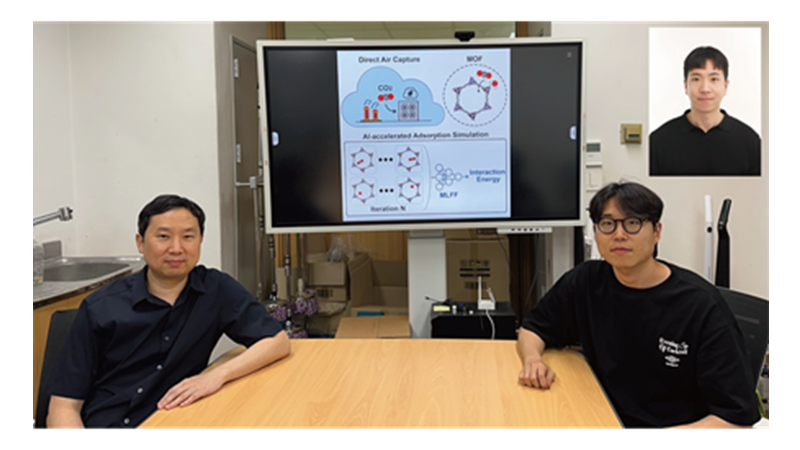
< Photo 1. (From left) Professor Jihan Kim, Ph.D. candidate Yunsung Lim and Dr. Hyunsoo Park of the Department of Chemical and Biomolecular Engineering >
In order to help prevent the climate crisis, actively reducing already-emitted CO₂ is essential. Accordingly, direct air capture (DAC) — a technology that directly extracts only CO₂ from the air — is gaining attention. However, effectively capturing pure CO₂ is not easy due to water vapor (H₂O) present in the air. KAIST researchers have successfully used AI-driven machine learning techniques to identify the most promising CO₂-capturing materials among metal-organic frameworks (MOFs), a key class of materials studied for this technology.
KAIST (President Kwang Hyung Lee) announced on the 29th of June that a research team led by Professor Jihan Kim from the Department of Chemical and Biomolecular Engineering, in collaboration with a team at Imperial College London, has developed a machine-learning-based simulation method that can quickly and accurately screen MOFs best suited for atmospheric CO₂ capture.
< Figure 1. Concept diagram of Direct Air Capture (DAC) technology and carbon capture using Metal-Organic Frameworks (MOFs). MOFs are promising porous materials capable of capturing carbon dioxide from the atmosphere, drawing attention as a core material for DAC technology. >
To overcome the difficulty of discovering high-performance materials due to the complexity of structures and the limitations of predicting intermolecular interactions, the research team developed a machine learning force field (MLFF) capable of precisely predicting the interactions between CO₂, water (H₂O), and MOFs. This new method enables calculations of MOF adsorption properties with quantum-mechanics-level accuracy at vastly faster speeds than before.
Using this system, the team screened over 8,000 experimentally synthesized MOF structures, identifying more than 100 promising candidates for CO₂ capture. Notably, this included new candidates that had not been uncovered by traditional force-field-based simulations. The team also analyzed the relationships between MOF chemical structure and adsorption performance, proposing seven key chemical features that will help in designing new materials for DAC.
< Figure 2. Concept diagram of adsorption simulation using Machine Learning Force Field (MLFF). The developed MLFF is applicable to various MOF structures and allows for precise calculation of adsorption properties by predicting interaction energies during repetitive Widom insertion simulations. It is characterized by simultaneously achieving high accuracy and low computational cost compared to conventional classical force fields. >
This research is recognized as a significant advance in the DAC field, greatly enhancing materials design and simulation by precisely predicting MOF-CO₂ and MOF-H₂O interactions.
The results of this research, with Ph.D. candidate Yunsung Lim and Dr. Hyunsoo Park of KAIST as co-first authors, were published in the international academic journal Matter on June 12.
※Paper Title: Accelerating CO₂ direct air capture screening for metal–organic frameworks with a transferable machine learning force field
※DOI: 10.1016/j.matt.2025.102203
This research was supported by the Saudi Aramco-KAIST CO₂ Management Center and the Ministry of Science and ICT's Global C.L.E.A.N. Project.
2025.06.29 View 134
KAIST Develops AI to Easily Find Promising Materials That Capture Only CO₂
< Photo 1. (From left) Professor Jihan Kim, Ph.D. candidate Yunsung Lim and Dr. Hyunsoo Park of the Department of Chemical and Biomolecular Engineering >
In order to help prevent the climate crisis, actively reducing already-emitted CO₂ is essential. Accordingly, direct air capture (DAC) — a technology that directly extracts only CO₂ from the air — is gaining attention. However, effectively capturing pure CO₂ is not easy due to water vapor (H₂O) present in the air. KAIST researchers have successfully used AI-driven machine learning techniques to identify the most promising CO₂-capturing materials among metal-organic frameworks (MOFs), a key class of materials studied for this technology.
KAIST (President Kwang Hyung Lee) announced on the 29th of June that a research team led by Professor Jihan Kim from the Department of Chemical and Biomolecular Engineering, in collaboration with a team at Imperial College London, has developed a machine-learning-based simulation method that can quickly and accurately screen MOFs best suited for atmospheric CO₂ capture.
< Figure 1. Concept diagram of Direct Air Capture (DAC) technology and carbon capture using Metal-Organic Frameworks (MOFs). MOFs are promising porous materials capable of capturing carbon dioxide from the atmosphere, drawing attention as a core material for DAC technology. >
To overcome the difficulty of discovering high-performance materials due to the complexity of structures and the limitations of predicting intermolecular interactions, the research team developed a machine learning force field (MLFF) capable of precisely predicting the interactions between CO₂, water (H₂O), and MOFs. This new method enables calculations of MOF adsorption properties with quantum-mechanics-level accuracy at vastly faster speeds than before.
Using this system, the team screened over 8,000 experimentally synthesized MOF structures, identifying more than 100 promising candidates for CO₂ capture. Notably, this included new candidates that had not been uncovered by traditional force-field-based simulations. The team also analyzed the relationships between MOF chemical structure and adsorption performance, proposing seven key chemical features that will help in designing new materials for DAC.
< Figure 2. Concept diagram of adsorption simulation using Machine Learning Force Field (MLFF). The developed MLFF is applicable to various MOF structures and allows for precise calculation of adsorption properties by predicting interaction energies during repetitive Widom insertion simulations. It is characterized by simultaneously achieving high accuracy and low computational cost compared to conventional classical force fields. >
This research is recognized as a significant advance in the DAC field, greatly enhancing materials design and simulation by precisely predicting MOF-CO₂ and MOF-H₂O interactions.
The results of this research, with Ph.D. candidate Yunsung Lim and Dr. Hyunsoo Park of KAIST as co-first authors, were published in the international academic journal Matter on June 12.
※Paper Title: Accelerating CO₂ direct air capture screening for metal–organic frameworks with a transferable machine learning force field
※DOI: 10.1016/j.matt.2025.102203
This research was supported by the Saudi Aramco-KAIST CO₂ Management Center and the Ministry of Science and ICT's Global C.L.E.A.N. Project.
2025.06.29 View 134 -
 New and Highly Efficient Recycling Technology to Turn Used Tires into Raw Materials for Rubber and Nylon
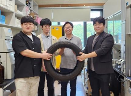
< (From left) Kyungmin Choi (MS-Ph.D. integrated course, Department of Chemistry), Dr. Beomsoon Park, Professor Soon Hyeok Hong, Dr. Kyoungil Cho >
Approximately 1.5 billions of tires are discarded globally every year, and this is identified as one of the major causes of serious environmental pollution. The research team at the Department of Chemistry at KAIST has achieved a breakthrough by selectively converting waste tires into high-purity cyclic alkenes, valuable chemical building blocks used in the production of rubber and nylon fibers. This advance marks a new milestone in chemical recycling technology for waste tires.
The team, led by Professor Soon Hyeok Hong, has developed a dual-catalyst-based reaction system that overcomes the long-standing challenges associated with recycling vulcanized rubber materials.
Tires are composed of complex blends of synthetic and natural rubber, and their physical strength and durability are reinforced with additives such as silica, carbon black, and antioxidants. In particular, cross-linking between rubber chains is formed through the vulcanization process, giving them a structure resistant to heat and pressure, which is one of the main reasons why chemical recycling of waste tires is difficult.
Until now, waste tire recycling has mainly relied on pyrolysis or mechanical recycling methods. The pyrolysis method is a technology that decomposes polymer chains at high temperatures of 350-800°C to convert them into fuel oil, but it clearly has limitations such as high energy consumption, low selectivity, and the production of low-quality hydrocarbon mixtures.
To solve these problems, the research team developed a method to convert waste rubber into useful chemicals using dual catalysis. The first catalyst helps to break down rubber molecules by changing their bonding structure, and the second catalyst creates cyclic compounds through a ring-closing reaction.
This process shows high selectivity of up to 92% and a yield of 82%. The produced cyclopentene can be recycled into rubber, and cyclohexene can be used as a raw material for nylon fibers, making them industrially very valuable.
The research team successfully applied the developed system to discarded waste tires, achieving selective conversion into high-purity cyclic alkenes. Unlike the existing pyrolysis method, this is evaluated as a new turning point in the field of waste tire recycling as it can produce high-value chemicals through low-temperature precision catalytic reactions.
In addition, this catalytic platform is compatible with a wide range of synthetic and waste rubbers, positioning it as a promising foundation for scalable, circular solutions in the polymer and materials industries.
< Figure 1. Development of a Catalytic Method for Chemical Recycling of Waste Rubber >
Professor Hong stated, "This research offers an innovative solution for the chemical recycling of waste tires. We aim to develop next-generation high-efficiency catalysts and lay the groundwork for commercialization to enhance economic feasibility. Ultimately, our goal is to contribute to solving the broader waste plastic problem through fundamental chemistry."
This research, in which Beomsoon Park, Kyoungil Cho, and Kyungmin Choi participated, was supported by the National Research Foundation of Korea and was published online in the internationally renowned academic journal ‘Chem’ on June 18th.
※Paper Title: Catalytic and Selective Chemical Recycling of Post-Consumer Rubbers into Cycloalkenes
※DOI: 10.1016/j.chempr.2025.102625
2025.06.26 View 493
New and Highly Efficient Recycling Technology to Turn Used Tires into Raw Materials for Rubber and Nylon
< (From left) Kyungmin Choi (MS-Ph.D. integrated course, Department of Chemistry), Dr. Beomsoon Park, Professor Soon Hyeok Hong, Dr. Kyoungil Cho >
Approximately 1.5 billions of tires are discarded globally every year, and this is identified as one of the major causes of serious environmental pollution. The research team at the Department of Chemistry at KAIST has achieved a breakthrough by selectively converting waste tires into high-purity cyclic alkenes, valuable chemical building blocks used in the production of rubber and nylon fibers. This advance marks a new milestone in chemical recycling technology for waste tires.
The team, led by Professor Soon Hyeok Hong, has developed a dual-catalyst-based reaction system that overcomes the long-standing challenges associated with recycling vulcanized rubber materials.
Tires are composed of complex blends of synthetic and natural rubber, and their physical strength and durability are reinforced with additives such as silica, carbon black, and antioxidants. In particular, cross-linking between rubber chains is formed through the vulcanization process, giving them a structure resistant to heat and pressure, which is one of the main reasons why chemical recycling of waste tires is difficult.
Until now, waste tire recycling has mainly relied on pyrolysis or mechanical recycling methods. The pyrolysis method is a technology that decomposes polymer chains at high temperatures of 350-800°C to convert them into fuel oil, but it clearly has limitations such as high energy consumption, low selectivity, and the production of low-quality hydrocarbon mixtures.
To solve these problems, the research team developed a method to convert waste rubber into useful chemicals using dual catalysis. The first catalyst helps to break down rubber molecules by changing their bonding structure, and the second catalyst creates cyclic compounds through a ring-closing reaction.
This process shows high selectivity of up to 92% and a yield of 82%. The produced cyclopentene can be recycled into rubber, and cyclohexene can be used as a raw material for nylon fibers, making them industrially very valuable.
The research team successfully applied the developed system to discarded waste tires, achieving selective conversion into high-purity cyclic alkenes. Unlike the existing pyrolysis method, this is evaluated as a new turning point in the field of waste tire recycling as it can produce high-value chemicals through low-temperature precision catalytic reactions.
In addition, this catalytic platform is compatible with a wide range of synthetic and waste rubbers, positioning it as a promising foundation for scalable, circular solutions in the polymer and materials industries.
< Figure 1. Development of a Catalytic Method for Chemical Recycling of Waste Rubber >
Professor Hong stated, "This research offers an innovative solution for the chemical recycling of waste tires. We aim to develop next-generation high-efficiency catalysts and lay the groundwork for commercialization to enhance economic feasibility. Ultimately, our goal is to contribute to solving the broader waste plastic problem through fundamental chemistry."
This research, in which Beomsoon Park, Kyoungil Cho, and Kyungmin Choi participated, was supported by the National Research Foundation of Korea and was published online in the internationally renowned academic journal ‘Chem’ on June 18th.
※Paper Title: Catalytic and Selective Chemical Recycling of Post-Consumer Rubbers into Cycloalkenes
※DOI: 10.1016/j.chempr.2025.102625
2025.06.26 View 493 -
 Military Combatants Usher in an Era of Personalized Training with New Materials
< Photo 1. (From left) Professor Steve Park of Materials Science and Engineering, Kyusoon Pak, Ph.D. Candidate (Army Major) >
Traditional military training often relies on standardized methods, which has limited the provision of optimized training tailored to individual combatants' characteristics or specific combat situations. To address this, our research team developed an e-textile platform, securing core technology that can reflect the unique traits of individual combatants and various combat scenarios. This technology has proven robust enough for battlefield use and is economical enough for widespread distribution to a large number of troops.
On June 25th, Professor Steve Park's research team at KAIST's Department of Materials Science and Engineering announced the development of a flexible, wearable electronic textile (E-textile) platform using an innovative technology that 'draws' electronic circuits directly onto fabric.
The wearable e-textile platform developed by the research team combines 3D printing technology with new materials engineering design to directly print flexible and highly durable sensors and electrodes onto textile substrates. This enables the collection of precise movement and human body data from individual combatants, which can then be used to propose customized training models.
Existing e-textile fabrication methods were often complex or limited in their ability to provide personalized customization. To overcome these challenges, the research team adopted an additive manufacturing technology called 'Direct Ink Writing (DIW)' 3D printing.
< Figure 1. Schematic diagram of e-textile manufactured with Direct Ink Writing (DIW) printing technology on various textiles, including combat uniforms >
This technology involves directly dispensing and printing special ink, which functions as sensors and electrodes, onto textile substrates in desired patterns. This allows for flexible implementation of various designs without the complex process of mask fabrication. This is expected to be an effective technology that can be easily supplied to hundreds of thousands of military personnel.
The core of this technology lies in the development of high-performance functional inks based on advanced materials engineering design. The research team combined styrene-butadiene-styrene (SBS) polymer, which provides flexibility, with multi-walled carbon nanotubes (MWCNT) for electrical conductivity. They developed a tensile/bending sensor ink that can stretch up to 102% and maintain stable performance even after 10,000 repetitive tests. This means that accurate data can be consistently obtained even during the strenuous movements of combatants.
< Figure 2. Measurement of human movement and breathing patterns using e-textile >
Furthermore, new material technology was applied to implement 'interconnect electrodes' that electrically connect the upper and lower layers of the fabric. The team developed an electrode ink combining silver (Ag) flakes with rigid polystyrene (PS) polymer, precisely controlling the impregnation level (how much the ink penetrates the fabric) to effectively connect both sides or multiple layers of the fabric. This secures the technology for producing multi-layered wearable electronic systems integrating sensors and electrodes.
< Figure 3. Experimental results of recognizing unknown objects after machine learning six objects using a smart glove >
The research team proved the platform's performance through actual human movement monitoring experiments. They printed the developed e-textile on major joint areas of clothing (shoulders, elbows, knees) and measured movements and posture changes during various exercises such as running, jumping jacks, and push-ups in real-time.
Additionally, they demonstrated the potential for applications such as monitoring breathing patterns using a smart mask and recognizing objects through machine learning and perceiving complex tactile information by printing multiple sensors and electrodes on gloves. These results show that the developed e-textile platform is effective in precisely understanding the movement dynamics of combatants.
This research is an important example demonstrating how cutting-edge new material technology can contribute to the advancement of the defense sector. Major Kyusoon Pak of the Army, who participated in this research, considered required objectives such as military applicability and economic feasibility for practical distribution from the research design stage.
< Figure 4. Experimental results showing that a multi-layered e-textile glove connected with interconnect electrodes can measure tensile/bending signals and pressure signals at a single point >
Major Pak stated, "Our military is currently facing both a crisis and an opportunity due to the decrease in military personnel resources caused by the demographic cliff and the advancement of science and technology. Also, respect for life in the battlefield is emerging as a significant issue. This research aims to secure original technology that can provide customized training according to military branch/duty and type of combat, thereby enhancing the combat power and ensuring the survivability of our soldiers."
He added, "I hope this research will be evaluated as a case that achieved both scientific contribution and military applicability."
This research, where Kyusoon Pak, Ph.D. Candidate (Army Major) from KAIST's Department of Materials Science and Engineering, participated as the first author and Professor Steve Park supervised, was published on May 27, 2025, in `npj Flexible Electronics (top 1.8% in JCR field)', an international academic journal in the electrical, electronic, and materials engineering fields.
* Paper Title: Fabrication of Multifunctional Wearable Interconnect E-textile Platform Using Direct Ink Writing (DIW) 3D Printing
* DOI: https://doi.org/10.1038/s41528-025-00414-7
This research was supported by the Ministry of Trade, Industry and Energy and the National Research Foundation of Korea.
2025.06.25 View 164
Military Combatants Usher in an Era of Personalized Training with New Materials
< Photo 1. (From left) Professor Steve Park of Materials Science and Engineering, Kyusoon Pak, Ph.D. Candidate (Army Major) >
Traditional military training often relies on standardized methods, which has limited the provision of optimized training tailored to individual combatants' characteristics or specific combat situations. To address this, our research team developed an e-textile platform, securing core technology that can reflect the unique traits of individual combatants and various combat scenarios. This technology has proven robust enough for battlefield use and is economical enough for widespread distribution to a large number of troops.
On June 25th, Professor Steve Park's research team at KAIST's Department of Materials Science and Engineering announced the development of a flexible, wearable electronic textile (E-textile) platform using an innovative technology that 'draws' electronic circuits directly onto fabric.
The wearable e-textile platform developed by the research team combines 3D printing technology with new materials engineering design to directly print flexible and highly durable sensors and electrodes onto textile substrates. This enables the collection of precise movement and human body data from individual combatants, which can then be used to propose customized training models.
Existing e-textile fabrication methods were often complex or limited in their ability to provide personalized customization. To overcome these challenges, the research team adopted an additive manufacturing technology called 'Direct Ink Writing (DIW)' 3D printing.
< Figure 1. Schematic diagram of e-textile manufactured with Direct Ink Writing (DIW) printing technology on various textiles, including combat uniforms >
This technology involves directly dispensing and printing special ink, which functions as sensors and electrodes, onto textile substrates in desired patterns. This allows for flexible implementation of various designs without the complex process of mask fabrication. This is expected to be an effective technology that can be easily supplied to hundreds of thousands of military personnel.
The core of this technology lies in the development of high-performance functional inks based on advanced materials engineering design. The research team combined styrene-butadiene-styrene (SBS) polymer, which provides flexibility, with multi-walled carbon nanotubes (MWCNT) for electrical conductivity. They developed a tensile/bending sensor ink that can stretch up to 102% and maintain stable performance even after 10,000 repetitive tests. This means that accurate data can be consistently obtained even during the strenuous movements of combatants.
< Figure 2. Measurement of human movement and breathing patterns using e-textile >
Furthermore, new material technology was applied to implement 'interconnect electrodes' that electrically connect the upper and lower layers of the fabric. The team developed an electrode ink combining silver (Ag) flakes with rigid polystyrene (PS) polymer, precisely controlling the impregnation level (how much the ink penetrates the fabric) to effectively connect both sides or multiple layers of the fabric. This secures the technology for producing multi-layered wearable electronic systems integrating sensors and electrodes.
< Figure 3. Experimental results of recognizing unknown objects after machine learning six objects using a smart glove >
The research team proved the platform's performance through actual human movement monitoring experiments. They printed the developed e-textile on major joint areas of clothing (shoulders, elbows, knees) and measured movements and posture changes during various exercises such as running, jumping jacks, and push-ups in real-time.
Additionally, they demonstrated the potential for applications such as monitoring breathing patterns using a smart mask and recognizing objects through machine learning and perceiving complex tactile information by printing multiple sensors and electrodes on gloves. These results show that the developed e-textile platform is effective in precisely understanding the movement dynamics of combatants.
This research is an important example demonstrating how cutting-edge new material technology can contribute to the advancement of the defense sector. Major Kyusoon Pak of the Army, who participated in this research, considered required objectives such as military applicability and economic feasibility for practical distribution from the research design stage.
< Figure 4. Experimental results showing that a multi-layered e-textile glove connected with interconnect electrodes can measure tensile/bending signals and pressure signals at a single point >
Major Pak stated, "Our military is currently facing both a crisis and an opportunity due to the decrease in military personnel resources caused by the demographic cliff and the advancement of science and technology. Also, respect for life in the battlefield is emerging as a significant issue. This research aims to secure original technology that can provide customized training according to military branch/duty and type of combat, thereby enhancing the combat power and ensuring the survivability of our soldiers."
He added, "I hope this research will be evaluated as a case that achieved both scientific contribution and military applicability."
This research, where Kyusoon Pak, Ph.D. Candidate (Army Major) from KAIST's Department of Materials Science and Engineering, participated as the first author and Professor Steve Park supervised, was published on May 27, 2025, in `npj Flexible Electronics (top 1.8% in JCR field)', an international academic journal in the electrical, electronic, and materials engineering fields.
* Paper Title: Fabrication of Multifunctional Wearable Interconnect E-textile Platform Using Direct Ink Writing (DIW) 3D Printing
* DOI: https://doi.org/10.1038/s41528-025-00414-7
This research was supported by the Ministry of Trade, Industry and Energy and the National Research Foundation of Korea.
2025.06.25 View 164 -
 KAIST's Li-Fi - Achieves 100 Times Faster Speed and Enhanced Security of Wi-Fi
- KAIST-KRISS Develop 'On-Device Encryption Optical Transmitter' Based on Eco-Friendly Quantum Dots
- New Li-Fi Platform Technology Achieves High Performance with 17.4% Device Efficiency and 29,000 nit Brightness, Simultaneously Improving Transmission Speed and Security
- Presents New Methodology for High-Speed and Encrypted Communication Through Single-Device-Based Dual-Channel Optical Modulation
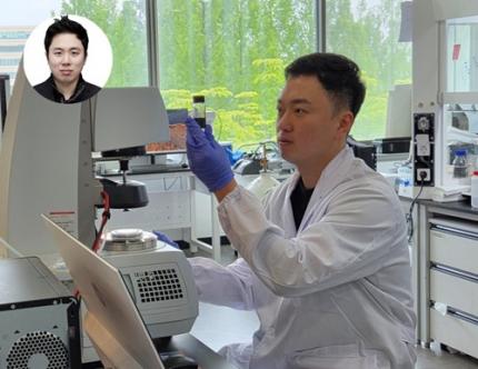
< Photo 1. (Front row from left) Seungmin Shin, First Author; Professor Himchan Cho; (Back row from left) Hyungdoh Lee, Seungwoo Lee, Wonbeom Lee; (Top left) Dr. Kyung-geun Lim >
Li-Fi (Light Fidelity) is a wireless communication technology that utilizes the visible light spectrum (400-800 THz), similar to LED light, offering speeds up to 100 times faster than existing Wi-Fi (up to 224 Gbps). While it has fewer limitations in available frequency allocation and less radio interference, it is relatively vulnerable to security breaches as anyone can access it. Korean researchers have now proposed a new Li-Fi platform that overcomes the limitations of conventional optical communication devices and can simultaneously enhance both transmission speed and security.
KAIST (President Kwang Hyung Lee) announced on the 24th that Professor Himchan Cho's research team from the Department of Materials Science and Engineering, in collaboration with Dr. Kyung-geun Lim of the Korea Research Institute of Standards and Science (KRISS, President Ho-Seong Lee) under the National Research Council of Science & Technology (NST, Chairman Young-Sik Kim), has developed 'on-device encryption optical communication device' technology for the utilization of 'Li-Fi,' which is attracting attention as a next-generation ultra-high-speed data communication.
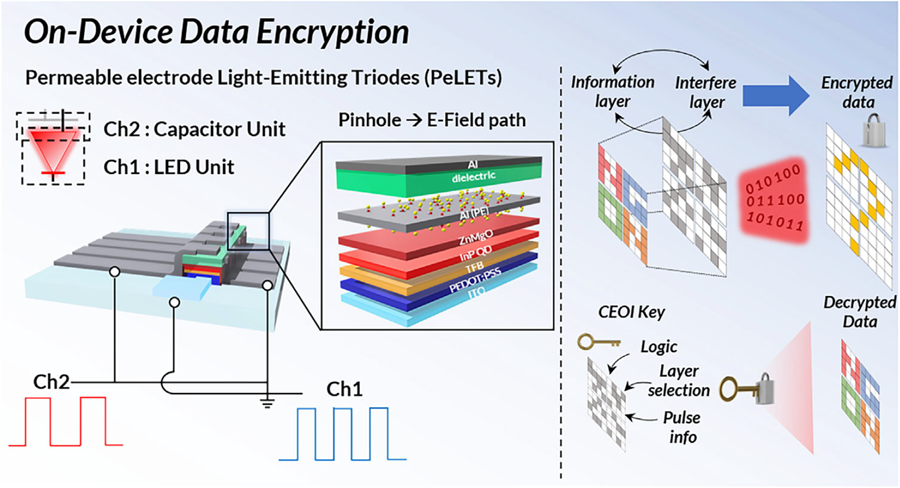
Professor Cho's team created high-efficiency light-emitting triode devices using eco-friendly quantum dots (low-toxicity and sustainable materials). The device developed by the research team is a mechanism that generates light using an electric field. Specifically, the electric field is concentrated in 'tiny holes (pinholes) in the permeable electrode' and transmitted beyond the electrode. This device utilizes this principle to simultaneously process two input data streams.
Using this principle, the research team developed a technology called 'on-device encryption optical transmitter.' The core of this technology is that the device itself converts information into light and simultaneously encrypts it. This means that enhanced security data transmission is possible without the need for complex, separate equipment.
External Quantum Efficiency (EQE) is an indicator of how efficiently electricity is converted into light, with a general commercialization standard of about 20%. The newly developed device recorded an EQE of 17.4%, and its luminance was 29,000 nit, significantly exceeding the maximum brightness of a smartphone OLED screen, which is 2,000 nit, demonstrating a brightness more than 10 times higher.
< Figure 1. Schematic diagram of the device structure developed by the research team and encrypted communication >
Furthermore, to more accurately understand how this device converts information into light, the research team used a method called 'transient electroluminescence analysis.' They analyzed the light-emitting characteristics generated by the device when voltage was instantaneously applied for very short durations (hundreds of nanoseconds = billionths of a second). Through this analysis, they investigated the movement of charges within the device at hundreds of nanoseconds, elucidating the operating mechanism of dual-channel optical modulation implemented within a single device.
Professor Himchan Cho of KAIST stated, "This research overcomes the limitations of existing optical communication devices and proposes a new communication platform that can both increase transmission speed and enhance security."
< Photo 2. Professor Himchan Cho, Department of Materials Science and Engineering >
He added, "This technology, which strengthens security without additional equipment and simultaneously enables encryption and transmission, can be widely applied in various fields where security is crucial in the future."
This research, with Seungmin Shin, a Ph.D. candidate at KAIST's Department of Materials Science and Engineering, participating as the first author, and Professor Himchan Cho and Dr. Kyung-geun Lim of KRISS as co-corresponding authors, was published in the international journal 'Advanced Materials' on May 30th and was selected as an inside front cover paper.※ Paper Title: High-Efficiency Quantum Dot Permeable electrode Light-Emitting Triodes for Visible-Light Communications and On-Device Data Encryption※ DOI: https://doi.org/10.1002/adma.202503189
This research was supported by the National Research Foundation of Korea, the National Research Council of Science & Technology (NST), and the Korea Institute for Advancement of Technology.
2025.06.24 View 586
KAIST's Li-Fi - Achieves 100 Times Faster Speed and Enhanced Security of Wi-Fi
- KAIST-KRISS Develop 'On-Device Encryption Optical Transmitter' Based on Eco-Friendly Quantum Dots
- New Li-Fi Platform Technology Achieves High Performance with 17.4% Device Efficiency and 29,000 nit Brightness, Simultaneously Improving Transmission Speed and Security
- Presents New Methodology for High-Speed and Encrypted Communication Through Single-Device-Based Dual-Channel Optical Modulation
< Photo 1. (Front row from left) Seungmin Shin, First Author; Professor Himchan Cho; (Back row from left) Hyungdoh Lee, Seungwoo Lee, Wonbeom Lee; (Top left) Dr. Kyung-geun Lim >
Li-Fi (Light Fidelity) is a wireless communication technology that utilizes the visible light spectrum (400-800 THz), similar to LED light, offering speeds up to 100 times faster than existing Wi-Fi (up to 224 Gbps). While it has fewer limitations in available frequency allocation and less radio interference, it is relatively vulnerable to security breaches as anyone can access it. Korean researchers have now proposed a new Li-Fi platform that overcomes the limitations of conventional optical communication devices and can simultaneously enhance both transmission speed and security.
KAIST (President Kwang Hyung Lee) announced on the 24th that Professor Himchan Cho's research team from the Department of Materials Science and Engineering, in collaboration with Dr. Kyung-geun Lim of the Korea Research Institute of Standards and Science (KRISS, President Ho-Seong Lee) under the National Research Council of Science & Technology (NST, Chairman Young-Sik Kim), has developed 'on-device encryption optical communication device' technology for the utilization of 'Li-Fi,' which is attracting attention as a next-generation ultra-high-speed data communication.
Professor Cho's team created high-efficiency light-emitting triode devices using eco-friendly quantum dots (low-toxicity and sustainable materials). The device developed by the research team is a mechanism that generates light using an electric field. Specifically, the electric field is concentrated in 'tiny holes (pinholes) in the permeable electrode' and transmitted beyond the electrode. This device utilizes this principle to simultaneously process two input data streams.
Using this principle, the research team developed a technology called 'on-device encryption optical transmitter.' The core of this technology is that the device itself converts information into light and simultaneously encrypts it. This means that enhanced security data transmission is possible without the need for complex, separate equipment.
External Quantum Efficiency (EQE) is an indicator of how efficiently electricity is converted into light, with a general commercialization standard of about 20%. The newly developed device recorded an EQE of 17.4%, and its luminance was 29,000 nit, significantly exceeding the maximum brightness of a smartphone OLED screen, which is 2,000 nit, demonstrating a brightness more than 10 times higher.
< Figure 1. Schematic diagram of the device structure developed by the research team and encrypted communication >
Furthermore, to more accurately understand how this device converts information into light, the research team used a method called 'transient electroluminescence analysis.' They analyzed the light-emitting characteristics generated by the device when voltage was instantaneously applied for very short durations (hundreds of nanoseconds = billionths of a second). Through this analysis, they investigated the movement of charges within the device at hundreds of nanoseconds, elucidating the operating mechanism of dual-channel optical modulation implemented within a single device.
Professor Himchan Cho of KAIST stated, "This research overcomes the limitations of existing optical communication devices and proposes a new communication platform that can both increase transmission speed and enhance security."
< Photo 2. Professor Himchan Cho, Department of Materials Science and Engineering >
He added, "This technology, which strengthens security without additional equipment and simultaneously enables encryption and transmission, can be widely applied in various fields where security is crucial in the future."
This research, with Seungmin Shin, a Ph.D. candidate at KAIST's Department of Materials Science and Engineering, participating as the first author, and Professor Himchan Cho and Dr. Kyung-geun Lim of KRISS as co-corresponding authors, was published in the international journal 'Advanced Materials' on May 30th and was selected as an inside front cover paper.※ Paper Title: High-Efficiency Quantum Dot Permeable electrode Light-Emitting Triodes for Visible-Light Communications and On-Device Data Encryption※ DOI: https://doi.org/10.1002/adma.202503189
This research was supported by the National Research Foundation of Korea, the National Research Council of Science & Technology (NST), and the Korea Institute for Advancement of Technology.
2025.06.24 View 586 -
 ‘InnoCORE Research Group’ Launched to Lead AI Convergence Innovation
KAIST announced on the 16th of June that it has launched the ‘InnoCORE (Innovation-Core) Research Group,’ which will lead advanced strategic research in AI convergence (AI+S&T), in cooperation with the Ministry of Science and ICT (Minister Yoo Sang-im, hereinafter referred to as MSIT) and DGIST, GIST, and UNIST*. Through this, the group plans to actively recruit up to 200 world-class postdoctoral researchers.
DGIST (Daegu Gyeongbuk Institute of Science & Technology), GIST (Gwangju Institute of Science & Technology), UNIST (Ulsan National Institute of Science and Technology)
The ‘InnoCORE Research Group’ aims to foster core research personnel who will lead innovation in the field of AI convergence, focusing on nurturing and attracting high-level research talent in AI+Science & Technology. This is a strategic response to prevent brain drain of domestic talent and attract excellent overseas talent amidst the accelerating global competition for AI talent.
Through this initiative, our university plans to accelerate AI-based science and technology innovation and disseminate research achievements across industries and the economy by supporting top domestic and international postdoctoral researchers to dedicate themselves to developing AI convergence technologies in an advanced collaborative research environment.
The InnoCORE project for advanced AI+S&T convergence research and global talent attraction is jointly promoted by four science and technology institutes, including KAIST. It is structured around AI core technologies (such as hyper-scale language models, AI semiconductors) and AI convergence technologies (such as bio, manufacturing, energy, and aerospace).
As the leading institution, our university operates the following four research groups:
Hyper-scale Language Model Innovation Research Group: Advancement of LLM technology and research on generative AI, multimodal AI, and ensuring reliability.
AI-based Intelligent Design-Manufacturing Integration Research Group: Establishment of an AI platform for the entire lifecycle of the manufacturing industry and innovation in design and processes.
AI-Innovation Drug Research Group: Securing AI-based drug development technologies across the entire lifecycle and overcoming intractable diseases.
AI-Transformed Aerospace Research Group: AI transformation of aerospace systems throughout their lifecycle and development of new technologies such as autonomous flight and space communication.
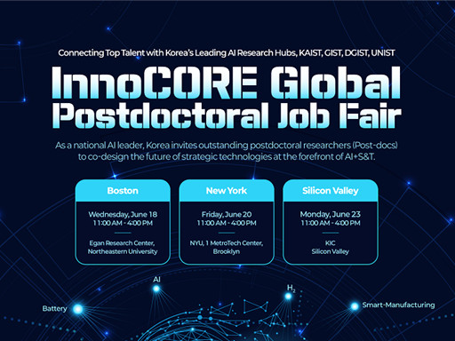
< Poster on the InnoCORE Global Jobfair for Recruitment of Postdoctoral Researchers >
In addition, a total of eight research groups are formed to promote global collaborative convergence research, including those led by DGIST, GIST, and UNIST: ▲Bio-Integrated Physical AI, ▲Early Diagnosis of Brain Diseases AI+Nano Convergence, ▲Intelligent Hydrogen Technology Innovation, and ▲AI-Space Solar Power Research Group.
Starting in 2025, the four science and technology institutes, including KAIST, will officially begin recruiting 400 postdoctoral researchers in the AI+S&T fields. Selected postdoctoral researchers will be guaranteed high-level treatment with an annual salary of over 90 million KRW, and additional support through matching with companies and research projects is also planned.
In particular, global recruitment fairs will be held in major US regions to expand the attraction of excellent overseas talent. Local recruitment fairs will be held in Boston (Harvard, MIT), New York (NYU), and Silicon Valley (Stanford) in June, along with promotions through global academic journals such as Nature and Science, and LinkedIn.
KAIST plans to provide multiple mentor programs, global joint research opportunities, and excellent infrastructure (such as supercomputers, semiconductor fabs, and AI research platforms) within the research groups to enable postdoctoral researchers to collaborate with experts from various academic and industrial fields.
President Kwang Hyung Lee emphasized, “Through this InnoCORE project, KAIST will leap forward as a Global Hub for AI+S&T convergence research. Young researchers from around the world will challenge themselves and grow at KAIST, and our country will play a pivotal role in establishing itself as a leading nation in global AI convergence research and industry. To achieve this, we will spare no effort in providing the best research environment and active support.”
KAIST plans to actively pursue the InnoCORE project to secure global competitiveness in AI convergence research and contribute to the development of advanced industries. The eight selected research groups will finalize their detailed research plans by the end of June and commence full-scale research in July.
2025.06.19 View 798
‘InnoCORE Research Group’ Launched to Lead AI Convergence Innovation
KAIST announced on the 16th of June that it has launched the ‘InnoCORE (Innovation-Core) Research Group,’ which will lead advanced strategic research in AI convergence (AI+S&T), in cooperation with the Ministry of Science and ICT (Minister Yoo Sang-im, hereinafter referred to as MSIT) and DGIST, GIST, and UNIST*. Through this, the group plans to actively recruit up to 200 world-class postdoctoral researchers.
DGIST (Daegu Gyeongbuk Institute of Science & Technology), GIST (Gwangju Institute of Science & Technology), UNIST (Ulsan National Institute of Science and Technology)
The ‘InnoCORE Research Group’ aims to foster core research personnel who will lead innovation in the field of AI convergence, focusing on nurturing and attracting high-level research talent in AI+Science & Technology. This is a strategic response to prevent brain drain of domestic talent and attract excellent overseas talent amidst the accelerating global competition for AI talent.
Through this initiative, our university plans to accelerate AI-based science and technology innovation and disseminate research achievements across industries and the economy by supporting top domestic and international postdoctoral researchers to dedicate themselves to developing AI convergence technologies in an advanced collaborative research environment.
The InnoCORE project for advanced AI+S&T convergence research and global talent attraction is jointly promoted by four science and technology institutes, including KAIST. It is structured around AI core technologies (such as hyper-scale language models, AI semiconductors) and AI convergence technologies (such as bio, manufacturing, energy, and aerospace).
As the leading institution, our university operates the following four research groups:
Hyper-scale Language Model Innovation Research Group: Advancement of LLM technology and research on generative AI, multimodal AI, and ensuring reliability.
AI-based Intelligent Design-Manufacturing Integration Research Group: Establishment of an AI platform for the entire lifecycle of the manufacturing industry and innovation in design and processes.
AI-Innovation Drug Research Group: Securing AI-based drug development technologies across the entire lifecycle and overcoming intractable diseases.
AI-Transformed Aerospace Research Group: AI transformation of aerospace systems throughout their lifecycle and development of new technologies such as autonomous flight and space communication.
< Poster on the InnoCORE Global Jobfair for Recruitment of Postdoctoral Researchers >
In addition, a total of eight research groups are formed to promote global collaborative convergence research, including those led by DGIST, GIST, and UNIST: ▲Bio-Integrated Physical AI, ▲Early Diagnosis of Brain Diseases AI+Nano Convergence, ▲Intelligent Hydrogen Technology Innovation, and ▲AI-Space Solar Power Research Group.
Starting in 2025, the four science and technology institutes, including KAIST, will officially begin recruiting 400 postdoctoral researchers in the AI+S&T fields. Selected postdoctoral researchers will be guaranteed high-level treatment with an annual salary of over 90 million KRW, and additional support through matching with companies and research projects is also planned.
In particular, global recruitment fairs will be held in major US regions to expand the attraction of excellent overseas talent. Local recruitment fairs will be held in Boston (Harvard, MIT), New York (NYU), and Silicon Valley (Stanford) in June, along with promotions through global academic journals such as Nature and Science, and LinkedIn.
KAIST plans to provide multiple mentor programs, global joint research opportunities, and excellent infrastructure (such as supercomputers, semiconductor fabs, and AI research platforms) within the research groups to enable postdoctoral researchers to collaborate with experts from various academic and industrial fields.
President Kwang Hyung Lee emphasized, “Through this InnoCORE project, KAIST will leap forward as a Global Hub for AI+S&T convergence research. Young researchers from around the world will challenge themselves and grow at KAIST, and our country will play a pivotal role in establishing itself as a leading nation in global AI convergence research and industry. To achieve this, we will spare no effort in providing the best research environment and active support.”
KAIST plans to actively pursue the InnoCORE project to secure global competitiveness in AI convergence research and contribute to the development of advanced industries. The eight selected research groups will finalize their detailed research plans by the end of June and commence full-scale research in July.
2025.06.19 View 798 -
 “One Experiment Is All It Takes”: KAIST Team Revolutionizes Drug Interaction Testing, Replacing 60,000 Studies
A groundbreaking new method developed by researchers at KAIST and Chungnam National University could drastically streamline drug interaction testing — replacing dozens of traditional experiments with just one.
The research, led by Professor Jae Kyoung Kim of KAIST Department of Mathematical Sciences & IBS Biomedical Mathematics Group and Professor Sang Kyum Kim of Chungnam National University's College of Pharmacy, introduces a novel analysis technique called 50-BOA, published in Nature Communications on June 5, 2025.
< Photo 1. (From left) Professor Sang Kyum Kim (Chungnam National University College of Pharmacy, co-corresponding author), Dr. Yun Min Song (IBS Biomedical Mathematics Group, formerly KAIST Department of Mathematical Sciences, co-first author), undergraduate student Hyeong Jun Jang (KAIST, co-first author), Professor Jae Kyoung Kim (KAIST and IBS Biomedical Mathematics Group, co-corresponding author) (Top left in the bubble) Professor Hwi-yeol Yun (Chungnam National University College of Pharmacy, co-author) >
For decades, scientists have had to repeat drug inhibition experiments across a wide range of concentrations to estimate inhibition constants — a process seen in over 60,000 scientific publications. But the KAIST-led team discovered that a single, well-chosen inhibitor concentration can yield even more accurate results.
< Figure 1. Graphical summary of 50-BOA. 50-BOA improves the accuracy and efficiency of inhibition constant estimation by using only a single inhibitor concentration instead of the traditionally used method of employing multiple inhibitor concentrations. >
“This approach challenges long-standing assumptions in experimental pharmacology,” says Prof. Kim. “It shows how mathematics can fundamentally redesign life science experiments.”
By mathematically analyzing the sources of error in conventional methods, the team found that over half the data typically collected adds no value or even skews results. Their new method not only cuts experimental effort by over 75%, but also enhances reproducibility and accuracy.
To help researchers adopt the method quickly, the team developed a user-friendly tool that takes simple Excel files as input, now freely available on GitHub:
☞ https://github.com/Mathbiomed/50-BOA
< Figure 2. The MATLAB and R package of 50-BOA at GitHub >
The work holds promise for faster and more reliable drug development, especially in assessing potential interactions in combination therapies. The U.S. FDA already emphasizes the importance of accurate enzyme inhibition assessment during early-stage drug evaluation — and this method could soon become a new gold standard.
2025.06.16 View 1191
“One Experiment Is All It Takes”: KAIST Team Revolutionizes Drug Interaction Testing, Replacing 60,000 Studies
A groundbreaking new method developed by researchers at KAIST and Chungnam National University could drastically streamline drug interaction testing — replacing dozens of traditional experiments with just one.
The research, led by Professor Jae Kyoung Kim of KAIST Department of Mathematical Sciences & IBS Biomedical Mathematics Group and Professor Sang Kyum Kim of Chungnam National University's College of Pharmacy, introduces a novel analysis technique called 50-BOA, published in Nature Communications on June 5, 2025.
< Photo 1. (From left) Professor Sang Kyum Kim (Chungnam National University College of Pharmacy, co-corresponding author), Dr. Yun Min Song (IBS Biomedical Mathematics Group, formerly KAIST Department of Mathematical Sciences, co-first author), undergraduate student Hyeong Jun Jang (KAIST, co-first author), Professor Jae Kyoung Kim (KAIST and IBS Biomedical Mathematics Group, co-corresponding author) (Top left in the bubble) Professor Hwi-yeol Yun (Chungnam National University College of Pharmacy, co-author) >
For decades, scientists have had to repeat drug inhibition experiments across a wide range of concentrations to estimate inhibition constants — a process seen in over 60,000 scientific publications. But the KAIST-led team discovered that a single, well-chosen inhibitor concentration can yield even more accurate results.
< Figure 1. Graphical summary of 50-BOA. 50-BOA improves the accuracy and efficiency of inhibition constant estimation by using only a single inhibitor concentration instead of the traditionally used method of employing multiple inhibitor concentrations. >
“This approach challenges long-standing assumptions in experimental pharmacology,” says Prof. Kim. “It shows how mathematics can fundamentally redesign life science experiments.”
By mathematically analyzing the sources of error in conventional methods, the team found that over half the data typically collected adds no value or even skews results. Their new method not only cuts experimental effort by over 75%, but also enhances reproducibility and accuracy.
To help researchers adopt the method quickly, the team developed a user-friendly tool that takes simple Excel files as input, now freely available on GitHub:
☞ https://github.com/Mathbiomed/50-BOA
< Figure 2. The MATLAB and R package of 50-BOA at GitHub >
The work holds promise for faster and more reliable drug development, especially in assessing potential interactions in combination therapies. The U.S. FDA already emphasizes the importance of accurate enzyme inhibition assessment during early-stage drug evaluation — and this method could soon become a new gold standard.
2025.06.16 View 1191 -
 High-Resolution Spectrometer that Fits into Smartphones Developed by KAIST Researchers
- Professor Mooseok Jang's research team at the Department of Bio and Brain Engineering develops an ultra-compact, high-resolution spectrometer using 'double-layer disordered metasurfaces' that generate unique random patterns depending on light's color.
- Unlike conventional dispersion-based spectrometers that were difficult to apply to portable devices, this new concept spectrometer technology achieves 1nm-level high resolution in a device smaller than 1cm, comparable in size to a fingernail.
- It can be utilized as a built-in spectrometer in smartphones and wearable devices in the future, and can be expanded to advanced optical technologies such as hyperspectral imaging and ultrafast imaging.
< Photo 1. (From left) Professor Mooseok Jang, Dong-gu Lee (Ph.D. candidate), Gookho Song (Ph.D. candidate) >
Color, as the way light's wavelength is perceived by the human eye, goes beyond a simple aesthetic element, containing important scientific information like a substance's composition or state. Spectrometers are optical devices that analyze material properties by decomposing light into its constituent wavelengths, and they are widely used in various scientific and industrial fields, including material analysis, chemical component detection, and life science research. Existing high-resolution spectrometers were large and complex, making them difficult for widespread daily use. However, thanks to the ultra-compact, high-resolution spectrometer developed by KAIST researchers, it is now expected that light's color information can be utilized even within smartphones or wearable devices.
KAIST (President Kwang Hyung Lee) announced on the 13th that Professor Mooseok Jang's research team at the Department of Bio and Brain Engineering has successfully developed a reconstruction-based spectrometer technology using double-layer disordered metasurfaces*.
*Double-layer disordered metasurface: An innovative optical device that complexly scatters light through two layers of disordered nanostructures, creating unique and predictable speckle patterns for each wavelength.
Existing high-resolution spectrometers have a large form factor, on the order of tens of centimeters, and require complex calibration processes to maintain accuracy. This fundamentally stems from the operating principle of traditional dispersive elements, such as gratings and prisms, which separate light wavelengths along the propagation direction, much like a rainbow separates colors. Consequently, despite the potential for light's color information to be widely useful in daily life, spectroscopic technology has been limited to laboratory or industrial manufacturing environments.
< Figure 1. Through a simple structure consisting of a double layer of disordered metasurfaces and an image sensor, it was shown that speckles of predictable spectral channels with high spectral resolution can be generated in a compact form factor. The high similarity between the measured and calculated speckles was used to solve the inverse problem and verify the ability to reconstruct the spectrum. >
The research team devised a method that departs from the conventional spectroscopic paradigm of using diffraction gratings or prisms, which establish a one-to-one correspondence between light's color information and its propagation direction, by utilizing designed disordered structures as optical components. In this process, they employed metasurfaces, which can freely control the light propagation process using structures tens to hundreds of nanometers in size, to accurately implement 'complex random patterns (speckle*)'.
*Speckle: An irregular pattern of light intensity created by the interference of multiple wavefronts of light.
Specifically, they developed a method that involves implementing a double-layer disordered metasurface to generate wavelength-specific speckle patterns and then reconstructing precise color information (wavelength) of the light from the random patterns measured by a camera.
As a result, they successfully developed a new concept spectrometer technology that can accurately measure light across a broad range of visible to infrared (440-1,300nm) with a high resolution of 1 nanometer (nm) in a device smaller than a fingernail (less than 1cm) using only a single image capture.
< Figure 2. A disordered metasurface is a metasurface with irregularly arranged structures ranging from tens to hundreds of nanometers in size. In a double-layer structure, a propagation space is placed between the two metasurfaces to control the output speckle with high degrees of freedom, thereby achieving a spectral resolution of 1 nm even in a form factor smaller than 1 cm. >
Dong-gu Lee, a lead author of this study, stated, "This technology is implemented in a way that is directly integrated with commercial image sensors, and we expect that it will enable easy acquisition and utilization of light's wavelength information in daily life when built into mobile devices in the future."
Professor Mooseok Jang said, "This technology overcomes the limitations of existing RGB three-color based machine vision fields, which only distinguish and recognize three color components (red, green, blue), and has diverse applications. We anticipate various applied research for this technology, which expands the horizon of laboratory-level technology to daily-level machine vision technology for applications such as food component analysis, crop health diagnosis, skin health measurement, environmental pollution detection, and bio/medical diagnostics." He added, "Furthermore, it can be extended to various advanced optical technologies such as hyperspectral imaging, which records wavelength and spatial information simultaneously with high resolution, 3D optical trapping technology, which precisely controls light of multiple wavelengths into desired forms, and ultrafast imaging technology, which captures phenomena occurring in very short periods."
This research was collaboratively led by Dong-gu Lee (Ph.D. candidate) and Gookho Song (Ph.D. candidate) from the KAIST Department of Bio and Brain Engineering as co-first authors, with Professor Mooseok Jang as the corresponding author. The findings were published online in the international journal Science Advances on May 28, 2025.* Paper Title: Reconstructive spectrometer using double-layer disordered metasurfaces* DOI: 10.1126/sciadv.adv2376
This research was supported by the Samsung Research Funding and Incubation Center of Samsung Electronics grant, the National Research Foundation of Korea (NRF) grant funded by the Korea government (MSIT), and the Bio & Medical Technology Development Program of the National Research Foundation (NRF) funded by the Korean government (MSIT).
2025.06.13 View 1111
High-Resolution Spectrometer that Fits into Smartphones Developed by KAIST Researchers
- Professor Mooseok Jang's research team at the Department of Bio and Brain Engineering develops an ultra-compact, high-resolution spectrometer using 'double-layer disordered metasurfaces' that generate unique random patterns depending on light's color.
- Unlike conventional dispersion-based spectrometers that were difficult to apply to portable devices, this new concept spectrometer technology achieves 1nm-level high resolution in a device smaller than 1cm, comparable in size to a fingernail.
- It can be utilized as a built-in spectrometer in smartphones and wearable devices in the future, and can be expanded to advanced optical technologies such as hyperspectral imaging and ultrafast imaging.
< Photo 1. (From left) Professor Mooseok Jang, Dong-gu Lee (Ph.D. candidate), Gookho Song (Ph.D. candidate) >
Color, as the way light's wavelength is perceived by the human eye, goes beyond a simple aesthetic element, containing important scientific information like a substance's composition or state. Spectrometers are optical devices that analyze material properties by decomposing light into its constituent wavelengths, and they are widely used in various scientific and industrial fields, including material analysis, chemical component detection, and life science research. Existing high-resolution spectrometers were large and complex, making them difficult for widespread daily use. However, thanks to the ultra-compact, high-resolution spectrometer developed by KAIST researchers, it is now expected that light's color information can be utilized even within smartphones or wearable devices.
KAIST (President Kwang Hyung Lee) announced on the 13th that Professor Mooseok Jang's research team at the Department of Bio and Brain Engineering has successfully developed a reconstruction-based spectrometer technology using double-layer disordered metasurfaces*.
*Double-layer disordered metasurface: An innovative optical device that complexly scatters light through two layers of disordered nanostructures, creating unique and predictable speckle patterns for each wavelength.
Existing high-resolution spectrometers have a large form factor, on the order of tens of centimeters, and require complex calibration processes to maintain accuracy. This fundamentally stems from the operating principle of traditional dispersive elements, such as gratings and prisms, which separate light wavelengths along the propagation direction, much like a rainbow separates colors. Consequently, despite the potential for light's color information to be widely useful in daily life, spectroscopic technology has been limited to laboratory or industrial manufacturing environments.
< Figure 1. Through a simple structure consisting of a double layer of disordered metasurfaces and an image sensor, it was shown that speckles of predictable spectral channels with high spectral resolution can be generated in a compact form factor. The high similarity between the measured and calculated speckles was used to solve the inverse problem and verify the ability to reconstruct the spectrum. >
The research team devised a method that departs from the conventional spectroscopic paradigm of using diffraction gratings or prisms, which establish a one-to-one correspondence between light's color information and its propagation direction, by utilizing designed disordered structures as optical components. In this process, they employed metasurfaces, which can freely control the light propagation process using structures tens to hundreds of nanometers in size, to accurately implement 'complex random patterns (speckle*)'.
*Speckle: An irregular pattern of light intensity created by the interference of multiple wavefronts of light.
Specifically, they developed a method that involves implementing a double-layer disordered metasurface to generate wavelength-specific speckle patterns and then reconstructing precise color information (wavelength) of the light from the random patterns measured by a camera.
As a result, they successfully developed a new concept spectrometer technology that can accurately measure light across a broad range of visible to infrared (440-1,300nm) with a high resolution of 1 nanometer (nm) in a device smaller than a fingernail (less than 1cm) using only a single image capture.
< Figure 2. A disordered metasurface is a metasurface with irregularly arranged structures ranging from tens to hundreds of nanometers in size. In a double-layer structure, a propagation space is placed between the two metasurfaces to control the output speckle with high degrees of freedom, thereby achieving a spectral resolution of 1 nm even in a form factor smaller than 1 cm. >
Dong-gu Lee, a lead author of this study, stated, "This technology is implemented in a way that is directly integrated with commercial image sensors, and we expect that it will enable easy acquisition and utilization of light's wavelength information in daily life when built into mobile devices in the future."
Professor Mooseok Jang said, "This technology overcomes the limitations of existing RGB three-color based machine vision fields, which only distinguish and recognize three color components (red, green, blue), and has diverse applications. We anticipate various applied research for this technology, which expands the horizon of laboratory-level technology to daily-level machine vision technology for applications such as food component analysis, crop health diagnosis, skin health measurement, environmental pollution detection, and bio/medical diagnostics." He added, "Furthermore, it can be extended to various advanced optical technologies such as hyperspectral imaging, which records wavelength and spatial information simultaneously with high resolution, 3D optical trapping technology, which precisely controls light of multiple wavelengths into desired forms, and ultrafast imaging technology, which captures phenomena occurring in very short periods."
This research was collaboratively led by Dong-gu Lee (Ph.D. candidate) and Gookho Song (Ph.D. candidate) from the KAIST Department of Bio and Brain Engineering as co-first authors, with Professor Mooseok Jang as the corresponding author. The findings were published online in the international journal Science Advances on May 28, 2025.* Paper Title: Reconstructive spectrometer using double-layer disordered metasurfaces* DOI: 10.1126/sciadv.adv2376
This research was supported by the Samsung Research Funding and Incubation Center of Samsung Electronics grant, the National Research Foundation of Korea (NRF) grant funded by the Korea government (MSIT), and the Bio & Medical Technology Development Program of the National Research Foundation (NRF) funded by the Korean government (MSIT).
2025.06.13 View 1111 -
 KAIST Turns an Unprecedented Idea into Reality: Quantum Computing with Magnets
What started as an idea under KAIST’s Global Singularity Research Project—"Can we build a quantum computer using magnets?"—has now become a scientific reality. A KAIST-led international research team has successfully demonstrated a core quantum computing technology using magnetic materials (ferromagnets) for the first time in the world.
KAIST (represented by President Kwang-Hyung Lee) announced on the 6th of May that a team led by Professor Kab-Jin Kim from the Department of Physics, in collaboration with the Argonne National Laboratory and the University of Illinois Urbana-Champaign (UIUC), has developed a “photon-magnon hybrid chip” and successfully implemented real-time, multi-pulse interference using magnetic materials—marking a global first.
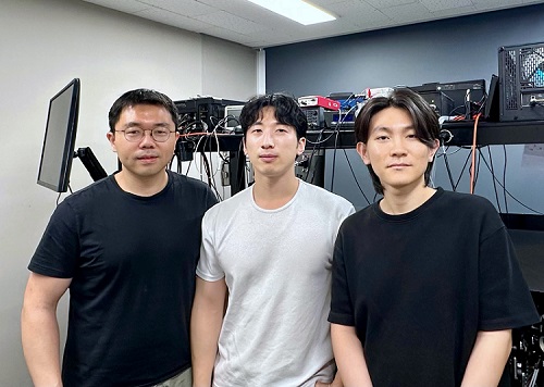
< Photo 1. Dr. Moojune Song (left) and Professor Kab-Jin Kim (right) of KAIST Department of Physics >
In simple terms, the researchers developed a special chip that synchronizes light and internal magnetic vibrations (magnons), enabling the transmission of phase information between distant magnets. They succeeded in observing and controlling interference between multiple signals in real time. This marks the first experimental evidence that magnets can serve as key components in quantum computing, serving as a pivotal step toward magnet-based quantum platforms.
The N and S poles of a magnet stem from the spin of electrons inside atoms. When many atoms align, their collective spin vibrations create a quantum particle known as a “magnon.”
Magnons are especially promising because of their nonreciprocal nature—they can carry information in only one direction, which makes them suitable for quantum noise isolation in compact quantum chips. They can also couple with both light and microwaves, enabling the potential for long-distance quantum communication over tens of kilometers.
Moreover, using special materials like antiferromagnets could allow quantum computers to operate at terahertz (THz) frequencies, far surpassing today’s hardware limitations, and possibly enabling room-temperature quantum computing without the need for bulky cryogenic equipment.
To build such a system, however, one must be able to transmit, measure, and control the phase information of magnons—the starting point and propagation of their waveforms—in real time. This had not been achieved until now.
< Figure 1. Superconducting Circuit-Based Magnon-Photon Hybrid System. (a) Schematic diagram of the device. A NbN superconducting resonator circuit fabricated on a silicon substrate is coupled with spherical YIG magnets (250 μm diameter), and magnons are generated and measured in real-time via a vertical antenna. (b) Photograph of the actual device. The distance between the two YIG spheres is 12 mm, a distance at which they cannot influence each other without the superconducting circuit. >
Professor Kim’s team used two tiny magnetic spheres made of Yttrium Iron Garnet (YIG) placed 12 mm apart with a superconducting resonator in between—similar to those used in quantum processors by Google and IBM. They input pulses into one magnet and successfully observed lossless transmission of magnon vibrations to the second magnet via the superconducting circuit.
They confirmed that from single nanosecond pulses to four microwave pulses, the magnon vibrations maintained their phase information and demonstrated predictable constructive or destructive interference in real time—known as coherent interference.
By adjusting the pulse frequencies and their intervals, the researchers could also freely control the interference patterns of magnons, effectively showing for the first time that electrical signals can be used to manipulate magnonic quantum states.
This work demonstrated that quantum gate operations using multiple pulses—a fundamental technique in quantum information processing—can be implemented using a hybrid system of magnetic materials and superconducting circuits. This opens the door for the practical use of magnet-based quantum devices.
< Figure 2. Experimental Data. (a) Measurement results of magnon-magnon band anticrossing via continuous wave measurement, showing the formation of a strong coupling hybrid system. (b) Magnon pulse exchange oscillation phenomenon between YIG spheres upon single pulse application. It can be seen that magnon information is coherently transmitted at regular time intervals through the superconducting circuit. (c,d) Magnon interference phenomenon upon dual pulse application. The magnon information state can be arbitrarily controlled by adjusting the time interval and carrier frequency between pulses. >
Professor Kab-Jin Kim stated, “This project began with a bold, even unconventional idea proposed to the Global Singularity Research Program: ‘What if we could build a quantum computer with magnets?’ The journey has been fascinating, and this study not only opens a new field of quantum spintronics, but also marks a turning point in developing high-efficiency quantum information processing devices.”
The research was co-led by postdoctoral researcher Moojune Song (KAIST), Dr. Yi Li and Dr. Valentine Novosad from Argonne National Lab, and Prof. Axel Hoffmann’s team at UIUC. The results were published in Nature Communications on April 17 and npj Spintronics on April 1, 2025.
Paper 1: Single-shot magnon interference in a magnon-superconducting-resonator hybrid circuit, Nat. Commun. 16, 3649 (2025)
DOI: https://doi.org/10.1038/s41467-025-58482-2
Paper 2: Single-shot electrical detection of short-wavelength magnon pulse transmission in a magnonic ultra-thin-film waveguide, npj Spintronics 3, 12 (2025)
DOI: https://doi.org/10.1038/s44306-025-00072-5
The research was supported by KAIST’s Global Singularity Research Initiative, the National Research Foundation of Korea (including the Mid-Career Researcher, Leading Research Center, and Quantum Information Science Human Resource Development programs), and the U.S. Department of Energy.
2025.06.12 View 1857
KAIST Turns an Unprecedented Idea into Reality: Quantum Computing with Magnets
What started as an idea under KAIST’s Global Singularity Research Project—"Can we build a quantum computer using magnets?"—has now become a scientific reality. A KAIST-led international research team has successfully demonstrated a core quantum computing technology using magnetic materials (ferromagnets) for the first time in the world.
KAIST (represented by President Kwang-Hyung Lee) announced on the 6th of May that a team led by Professor Kab-Jin Kim from the Department of Physics, in collaboration with the Argonne National Laboratory and the University of Illinois Urbana-Champaign (UIUC), has developed a “photon-magnon hybrid chip” and successfully implemented real-time, multi-pulse interference using magnetic materials—marking a global first.
< Photo 1. Dr. Moojune Song (left) and Professor Kab-Jin Kim (right) of KAIST Department of Physics >
In simple terms, the researchers developed a special chip that synchronizes light and internal magnetic vibrations (magnons), enabling the transmission of phase information between distant magnets. They succeeded in observing and controlling interference between multiple signals in real time. This marks the first experimental evidence that magnets can serve as key components in quantum computing, serving as a pivotal step toward magnet-based quantum platforms.
The N and S poles of a magnet stem from the spin of electrons inside atoms. When many atoms align, their collective spin vibrations create a quantum particle known as a “magnon.”
Magnons are especially promising because of their nonreciprocal nature—they can carry information in only one direction, which makes them suitable for quantum noise isolation in compact quantum chips. They can also couple with both light and microwaves, enabling the potential for long-distance quantum communication over tens of kilometers.
Moreover, using special materials like antiferromagnets could allow quantum computers to operate at terahertz (THz) frequencies, far surpassing today’s hardware limitations, and possibly enabling room-temperature quantum computing without the need for bulky cryogenic equipment.
To build such a system, however, one must be able to transmit, measure, and control the phase information of magnons—the starting point and propagation of their waveforms—in real time. This had not been achieved until now.
< Figure 1. Superconducting Circuit-Based Magnon-Photon Hybrid System. (a) Schematic diagram of the device. A NbN superconducting resonator circuit fabricated on a silicon substrate is coupled with spherical YIG magnets (250 μm diameter), and magnons are generated and measured in real-time via a vertical antenna. (b) Photograph of the actual device. The distance between the two YIG spheres is 12 mm, a distance at which they cannot influence each other without the superconducting circuit. >
Professor Kim’s team used two tiny magnetic spheres made of Yttrium Iron Garnet (YIG) placed 12 mm apart with a superconducting resonator in between—similar to those used in quantum processors by Google and IBM. They input pulses into one magnet and successfully observed lossless transmission of magnon vibrations to the second magnet via the superconducting circuit.
They confirmed that from single nanosecond pulses to four microwave pulses, the magnon vibrations maintained their phase information and demonstrated predictable constructive or destructive interference in real time—known as coherent interference.
By adjusting the pulse frequencies and their intervals, the researchers could also freely control the interference patterns of magnons, effectively showing for the first time that electrical signals can be used to manipulate magnonic quantum states.
This work demonstrated that quantum gate operations using multiple pulses—a fundamental technique in quantum information processing—can be implemented using a hybrid system of magnetic materials and superconducting circuits. This opens the door for the practical use of magnet-based quantum devices.
< Figure 2. Experimental Data. (a) Measurement results of magnon-magnon band anticrossing via continuous wave measurement, showing the formation of a strong coupling hybrid system. (b) Magnon pulse exchange oscillation phenomenon between YIG spheres upon single pulse application. It can be seen that magnon information is coherently transmitted at regular time intervals through the superconducting circuit. (c,d) Magnon interference phenomenon upon dual pulse application. The magnon information state can be arbitrarily controlled by adjusting the time interval and carrier frequency between pulses. >
Professor Kab-Jin Kim stated, “This project began with a bold, even unconventional idea proposed to the Global Singularity Research Program: ‘What if we could build a quantum computer with magnets?’ The journey has been fascinating, and this study not only opens a new field of quantum spintronics, but also marks a turning point in developing high-efficiency quantum information processing devices.”
The research was co-led by postdoctoral researcher Moojune Song (KAIST), Dr. Yi Li and Dr. Valentine Novosad from Argonne National Lab, and Prof. Axel Hoffmann’s team at UIUC. The results were published in Nature Communications on April 17 and npj Spintronics on April 1, 2025.
Paper 1: Single-shot magnon interference in a magnon-superconducting-resonator hybrid circuit, Nat. Commun. 16, 3649 (2025)
DOI: https://doi.org/10.1038/s41467-025-58482-2
Paper 2: Single-shot electrical detection of short-wavelength magnon pulse transmission in a magnonic ultra-thin-film waveguide, npj Spintronics 3, 12 (2025)
DOI: https://doi.org/10.1038/s44306-025-00072-5
The research was supported by KAIST’s Global Singularity Research Initiative, the National Research Foundation of Korea (including the Mid-Career Researcher, Leading Research Center, and Quantum Information Science Human Resource Development programs), and the U.S. Department of Energy.
2025.06.12 View 1857 -
 KAIST Successfully Develops High-Performance Water Electrolysis Without Platinum, Bringing Hydrogen Economy Closer
< Photo 1. (Front row, from left) Jeesoo Park (Ph.D. Candidate), Professor Hee-Tak Kim (Back row, from left) Kyunghwa Seok (Ph.D. Candidate), Dr. Gisu Doo, Euntaek Oh (Ph.D. Candidate) >
Hydrogen is gaining attention as a clean energy source that emits no carbon. Among various methods, water electrolysis, which splits water into hydrogen and oxygen using electricity, is recognized as an eco-friendly hydrogen production method. Specifically, proton exchange membrane water electrolysis (PEMWE) is considered a next-generation hydrogen production technology due to its ability to produce high-purity hydrogen at high pressure. However, existing PEMWE technology has faced limitations in commercialization due to its heavy reliance on expensive precious metal catalysts and coating materials. Korean researchers have now proposed a new solution to address these technical and economic bottlenecks.
KAIST (President Kwang Hyung Lee) announced on June 11th that a research team led by Professor Hee-Tak Kim of the Department of Chemical and Biomolecular Engineering, in a joint study with Dr. Gisu Doo of the Korea Institute of Energy Research (KIER, President Chang-keun Lee), has developed a next-generation water electrolysis technology that achieves high performance without the need for expensive platinum (Pt) coating.
The research team focused on the primary reason why 'iridium oxide (IrOx),' a highly active catalyst for water electrolysis electrodes, fails to perform optimally. They found that this is due to inefficient electron transfer and, for the first time in the world, demonstrated that performance can be maximized simply by controlling the catalyst particle size.
In this study, it was revealed that the reason iridium oxide catalysts do not exhibit excellent performance without platinum coating is due to 'electron transport resistance' that occurs at the interface between the catalyst, the ion conductor (hereinafter referred to as ionomer), and the Ti (titanium) substrate—core components inherently used together in water electrolysis electrodes.
Specifically, they identified that the 'pinch-off' phenomenon, where the electron pathway is blocked between the catalyst, ionomer, and titanium substrate, is the critical cause of reduced conductivity. The ionomer has properties close to an electron insulator, thereby hindering electron flow when it surrounds catalyst particles. Furthermore, when the ionomer comes into contact with the titanium substrate, an electron barrier forms on the surface oxide layer of the titanium substrate, significantly increasing resistance.
< Figure 1. Infographic related to electron transport resistance at the catalyst layer/diffusion layer interface >
To address this, the research team fabricated and compared catalysts of various particle sizes. Through single-cell evaluation and multiphysics simulations, they demonstrated, for the first time globally, that when iridium oxide catalyst particles with a size of 20 nanometers (nm) or larger are used, the ionomer mixed region decreases, ensuring an electron pathway and restoring conductivity.
Moreover, they successfully optimized the interfacial structure through precise design, simultaneously ensuring both reactivity and electron transport. This achievement demonstrated that the previously unavoidable trade-off between catalyst activity and conductivity can be overcome through meticulous interfacial design.
This breakthrough is expected to be a significant milestone not only for the development of high-performance catalyst materials but also for the future commercialization of proton exchange membrane water electrolysis systems that can achieve high efficiency while drastically reducing the amount of precious metals used.
Professor Hee-Tak Kim stated, "This research presents a new interface design strategy that can resolve the interfacial conductivity problem, which was a bottleneck in high-performance water electrolysis technology." He added, "By securing high performance even without expensive materials like platinum, it will be a stepping stone closer to realizing a hydrogen economy."
This research, with Jeesoo Park, a Ph.D. student from the Department of Chemical and Biomolecular Engineering at KAIST, as the first author, was published on June 7th in 'Energy & Environmental Science' (IF: 32.4, 2025), a leading international journal in the energy and environmental fields, and was recognized for its innovativeness and impact. (Paper title: On the interface electron transport problem of highly active IrOx catalysts, DOI: 10.1039/D4EE05816J).
This research was supported by the New and Renewable Energy Core Technology Development Project of the Ministry of Trade, Industry and Energy.
2025.06.11 View 1506
KAIST Successfully Develops High-Performance Water Electrolysis Without Platinum, Bringing Hydrogen Economy Closer
< Photo 1. (Front row, from left) Jeesoo Park (Ph.D. Candidate), Professor Hee-Tak Kim (Back row, from left) Kyunghwa Seok (Ph.D. Candidate), Dr. Gisu Doo, Euntaek Oh (Ph.D. Candidate) >
Hydrogen is gaining attention as a clean energy source that emits no carbon. Among various methods, water electrolysis, which splits water into hydrogen and oxygen using electricity, is recognized as an eco-friendly hydrogen production method. Specifically, proton exchange membrane water electrolysis (PEMWE) is considered a next-generation hydrogen production technology due to its ability to produce high-purity hydrogen at high pressure. However, existing PEMWE technology has faced limitations in commercialization due to its heavy reliance on expensive precious metal catalysts and coating materials. Korean researchers have now proposed a new solution to address these technical and economic bottlenecks.
KAIST (President Kwang Hyung Lee) announced on June 11th that a research team led by Professor Hee-Tak Kim of the Department of Chemical and Biomolecular Engineering, in a joint study with Dr. Gisu Doo of the Korea Institute of Energy Research (KIER, President Chang-keun Lee), has developed a next-generation water electrolysis technology that achieves high performance without the need for expensive platinum (Pt) coating.
The research team focused on the primary reason why 'iridium oxide (IrOx),' a highly active catalyst for water electrolysis electrodes, fails to perform optimally. They found that this is due to inefficient electron transfer and, for the first time in the world, demonstrated that performance can be maximized simply by controlling the catalyst particle size.
In this study, it was revealed that the reason iridium oxide catalysts do not exhibit excellent performance without platinum coating is due to 'electron transport resistance' that occurs at the interface between the catalyst, the ion conductor (hereinafter referred to as ionomer), and the Ti (titanium) substrate—core components inherently used together in water electrolysis electrodes.
Specifically, they identified that the 'pinch-off' phenomenon, where the electron pathway is blocked between the catalyst, ionomer, and titanium substrate, is the critical cause of reduced conductivity. The ionomer has properties close to an electron insulator, thereby hindering electron flow when it surrounds catalyst particles. Furthermore, when the ionomer comes into contact with the titanium substrate, an electron barrier forms on the surface oxide layer of the titanium substrate, significantly increasing resistance.
< Figure 1. Infographic related to electron transport resistance at the catalyst layer/diffusion layer interface >
To address this, the research team fabricated and compared catalysts of various particle sizes. Through single-cell evaluation and multiphysics simulations, they demonstrated, for the first time globally, that when iridium oxide catalyst particles with a size of 20 nanometers (nm) or larger are used, the ionomer mixed region decreases, ensuring an electron pathway and restoring conductivity.
Moreover, they successfully optimized the interfacial structure through precise design, simultaneously ensuring both reactivity and electron transport. This achievement demonstrated that the previously unavoidable trade-off between catalyst activity and conductivity can be overcome through meticulous interfacial design.
This breakthrough is expected to be a significant milestone not only for the development of high-performance catalyst materials but also for the future commercialization of proton exchange membrane water electrolysis systems that can achieve high efficiency while drastically reducing the amount of precious metals used.
Professor Hee-Tak Kim stated, "This research presents a new interface design strategy that can resolve the interfacial conductivity problem, which was a bottleneck in high-performance water electrolysis technology." He added, "By securing high performance even without expensive materials like platinum, it will be a stepping stone closer to realizing a hydrogen economy."
This research, with Jeesoo Park, a Ph.D. student from the Department of Chemical and Biomolecular Engineering at KAIST, as the first author, was published on June 7th in 'Energy & Environmental Science' (IF: 32.4, 2025), a leading international journal in the energy and environmental fields, and was recognized for its innovativeness and impact. (Paper title: On the interface electron transport problem of highly active IrOx catalysts, DOI: 10.1039/D4EE05816J).
This research was supported by the New and Renewable Energy Core Technology Development Project of the Ministry of Trade, Industry and Energy.
2025.06.11 View 1506 -
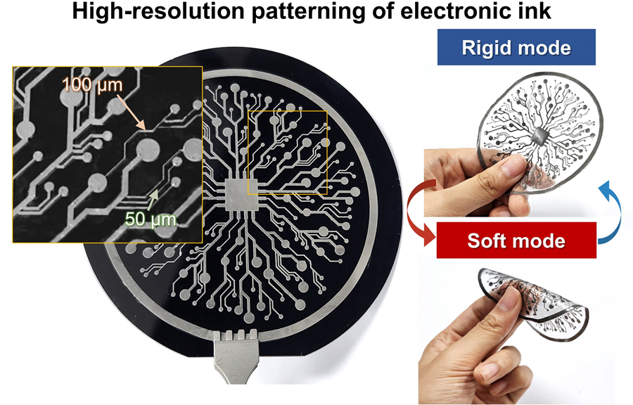 KAIST Research Team Develops Electronic Ink for Room-Temperature Printing of High-Resolution, Variable-Stiffness Electronics
A team of researchers from KAIST and Seoul National University has developed a groundbreaking electronic ink that enables room-temperature printing of variable-stiffness circuits capable of switching between rigid and soft modes. This advancement marks a significant leap toward next-generation wearable, implantable, and robotic devices.
< Photo 1. (From left) Professor Jae-Woong Jeong and PhD candidate Simok Lee of the School of Electrical Engineering, (in separate bubbles, from left) Professor Gun-Hee Lee of Pusan National University, Professor Seongjun Park of Seoul National University, Professor Steve Park of the Department of Materials Science and Engineering>
Variable-stiffness electronics are at the forefront of adaptive technology, offering the ability for a single device to transition between rigid and soft modes depending on its use case. Gallium, a metal known for its high rigidity contrast between solid and liquid states, is a promising candidate for such applications. However, its use has been hindered by challenges including high surface tension, low viscosity, and undesirable phase transitions during manufacturing.
On June 4th, a research team led by Professor Jae-Woong Jeong from the School of Electrical Engineering at KAIST, Professor Seongjun Park from the Digital Healthcare Major at Seoul National University, and Professor Steve Park from the Department of Materials Science and Engineering at KAIST introduced a novel liquid metal electronic ink. This ink allows for micro-scale circuit printing – thinner than a human hair – at room temperature, with the ability to reversibly switch between rigid and soft modes depending on temperature.
The new ink combines printable viscosity with excellent electrical conductivity, enabling the creation of complex, high-resolution multilayer circuits comparable to commercial printed circuit boards (PCBs). These circuits can dynamically change stiffness in response to temperature, presenting new opportunities for multifunctional electronics, medical technologies, and robotics.
Conventional electronics typically have fixed form factors – either rigid for durability or soft for wearability. Rigid devices like smartphones and laptops offer robust performance but are uncomfortable when worn, while soft electronics are more comfortable but lack precise handling. As demand grows for devices that can adapt their stiffness to context, variable-stiffness electronics are becoming increasingly important.
< Figure 1. Fabrication process of stable, high-viscosity electronic ink by dispersing micro-sized gallium particles in a polymer matrix (left). High-resolution large-area circuit printing process through pH-controlled chemical sintering (right). >
To address this challenge, the researchers focused on gallium, which melts just below body temperature. Solid gallium is quite stiff, while its liquid form is fluid and soft. Despite its potential, gallium’s use in electronic printing has been limited by its high surface tension and instability when melted.
To overcome these issues, the team developed a pH-controlled liquid metal ink printing process. By dispersing micro-sized gallium particles into a hydrophilic polyurethane matrix using a neutral solvent (dimethyl sulfoxide, or DMSO), they created a stable, high-viscosity ink suitable for precision printing. During post-print heating, the DMSO decomposes to form an acidic environment, which removes the oxide layer on the gallium particles. This triggers the particles to coalesce into electrically conductive networks with tunable mechanical properties.
The resulting printed circuits exhibit fine feature sizes (~50 μm), high conductivity (2.27 × 10⁶ S/m), and a stiffness modulation ratio of up to 1,465 – allowing the material to shift from plastic-like rigidity to rubber-like softness. Furthermore, the ink is compatible with conventional printing techniques such as screen printing and dip coating, supporting large-area and 3D device fabrication.
< Figure 2. Key features of the electronic ink. (i) High-resolution printing and multilayer integration capability. (ii) Batch fabrication capability through large-area screen printing. (iii) Complex three-dimensional structure printing capability through dip coating. (iv) Excellent electrical conductivity and stiffness control capability.>
The team demonstrated this technology by developing a multi-functional device that operates as a rigid portable electronic under normal conditions but transforms into a soft wearable healthcare device when attached to the body. They also created a neural probe that remains stiff during surgical insertion for accurate positioning but softens once inside brain tissue to reduce inflammation – highlighting its potential for biomedical implants.
< Figure 3. Variable stiffness wearable electronics with high-resolution circuits and multilayer structure comparable to commercial printed circuit boards (PCBs). Functions as a rigid portable electronic device at room temperature, then transforms into a wearable healthcare device by softening at body temperature upon skin contact.>
“The core achievement of this research lies in overcoming the longstanding challenges of liquid metal printing through our innovative technology,” said Professor Jeong. “By controlling the ink’s acidity, we were able to electrically and mechanically connect printed gallium particles, enabling the room-temperature fabrication of high-resolution, large-area circuits with tunable stiffness. This opens up new possibilities for future personal electronics, medical devices, and robotics.”
< Figure 4. Body-temperature softening neural probe implemented by coating electronic ink on an optical waveguide structure. (Left) Remains rigid during surgery for precise manipulation and brain insertion, then softens after implantation to minimize mechanical stress on the brain and greatly enhance biocompatibility. (Right) >
This research was published in Science Advances under the title, “Phase-Change Metal Ink with pH-Controlled Chemical Sintering for Versatile and Scalable Fabrication of Variable Stiffness Electronics.” The work was supported by the National Research Foundation of Korea, the Boston-Korea Project, and the BK21 FOUR Program.
2025.06.04 View 1857
KAIST Research Team Develops Electronic Ink for Room-Temperature Printing of High-Resolution, Variable-Stiffness Electronics
A team of researchers from KAIST and Seoul National University has developed a groundbreaking electronic ink that enables room-temperature printing of variable-stiffness circuits capable of switching between rigid and soft modes. This advancement marks a significant leap toward next-generation wearable, implantable, and robotic devices.
< Photo 1. (From left) Professor Jae-Woong Jeong and PhD candidate Simok Lee of the School of Electrical Engineering, (in separate bubbles, from left) Professor Gun-Hee Lee of Pusan National University, Professor Seongjun Park of Seoul National University, Professor Steve Park of the Department of Materials Science and Engineering>
Variable-stiffness electronics are at the forefront of adaptive technology, offering the ability for a single device to transition between rigid and soft modes depending on its use case. Gallium, a metal known for its high rigidity contrast between solid and liquid states, is a promising candidate for such applications. However, its use has been hindered by challenges including high surface tension, low viscosity, and undesirable phase transitions during manufacturing.
On June 4th, a research team led by Professor Jae-Woong Jeong from the School of Electrical Engineering at KAIST, Professor Seongjun Park from the Digital Healthcare Major at Seoul National University, and Professor Steve Park from the Department of Materials Science and Engineering at KAIST introduced a novel liquid metal electronic ink. This ink allows for micro-scale circuit printing – thinner than a human hair – at room temperature, with the ability to reversibly switch between rigid and soft modes depending on temperature.
The new ink combines printable viscosity with excellent electrical conductivity, enabling the creation of complex, high-resolution multilayer circuits comparable to commercial printed circuit boards (PCBs). These circuits can dynamically change stiffness in response to temperature, presenting new opportunities for multifunctional electronics, medical technologies, and robotics.
Conventional electronics typically have fixed form factors – either rigid for durability or soft for wearability. Rigid devices like smartphones and laptops offer robust performance but are uncomfortable when worn, while soft electronics are more comfortable but lack precise handling. As demand grows for devices that can adapt their stiffness to context, variable-stiffness electronics are becoming increasingly important.
< Figure 1. Fabrication process of stable, high-viscosity electronic ink by dispersing micro-sized gallium particles in a polymer matrix (left). High-resolution large-area circuit printing process through pH-controlled chemical sintering (right). >
To address this challenge, the researchers focused on gallium, which melts just below body temperature. Solid gallium is quite stiff, while its liquid form is fluid and soft. Despite its potential, gallium’s use in electronic printing has been limited by its high surface tension and instability when melted.
To overcome these issues, the team developed a pH-controlled liquid metal ink printing process. By dispersing micro-sized gallium particles into a hydrophilic polyurethane matrix using a neutral solvent (dimethyl sulfoxide, or DMSO), they created a stable, high-viscosity ink suitable for precision printing. During post-print heating, the DMSO decomposes to form an acidic environment, which removes the oxide layer on the gallium particles. This triggers the particles to coalesce into electrically conductive networks with tunable mechanical properties.
The resulting printed circuits exhibit fine feature sizes (~50 μm), high conductivity (2.27 × 10⁶ S/m), and a stiffness modulation ratio of up to 1,465 – allowing the material to shift from plastic-like rigidity to rubber-like softness. Furthermore, the ink is compatible with conventional printing techniques such as screen printing and dip coating, supporting large-area and 3D device fabrication.
< Figure 2. Key features of the electronic ink. (i) High-resolution printing and multilayer integration capability. (ii) Batch fabrication capability through large-area screen printing. (iii) Complex three-dimensional structure printing capability through dip coating. (iv) Excellent electrical conductivity and stiffness control capability.>
The team demonstrated this technology by developing a multi-functional device that operates as a rigid portable electronic under normal conditions but transforms into a soft wearable healthcare device when attached to the body. They also created a neural probe that remains stiff during surgical insertion for accurate positioning but softens once inside brain tissue to reduce inflammation – highlighting its potential for biomedical implants.
< Figure 3. Variable stiffness wearable electronics with high-resolution circuits and multilayer structure comparable to commercial printed circuit boards (PCBs). Functions as a rigid portable electronic device at room temperature, then transforms into a wearable healthcare device by softening at body temperature upon skin contact.>
“The core achievement of this research lies in overcoming the longstanding challenges of liquid metal printing through our innovative technology,” said Professor Jeong. “By controlling the ink’s acidity, we were able to electrically and mechanically connect printed gallium particles, enabling the room-temperature fabrication of high-resolution, large-area circuits with tunable stiffness. This opens up new possibilities for future personal electronics, medical devices, and robotics.”
< Figure 4. Body-temperature softening neural probe implemented by coating electronic ink on an optical waveguide structure. (Left) Remains rigid during surgery for precise manipulation and brain insertion, then softens after implantation to minimize mechanical stress on the brain and greatly enhance biocompatibility. (Right) >
This research was published in Science Advances under the title, “Phase-Change Metal Ink with pH-Controlled Chemical Sintering for Versatile and Scalable Fabrication of Variable Stiffness Electronics.” The work was supported by the National Research Foundation of Korea, the Boston-Korea Project, and the BK21 FOUR Program.
2025.06.04 View 1857 -
 RAIBO Runs over Walls with Feline Agility... Ready for Effortless Search over Mountaineous and Rough Terrains
< Photo 1. Research Team Photo (Professor Jemin Hwangbo, second from right in the front row) >
KAIST's quadrupedal robot, RAIBO, can now move at high speed across discontinuous and complex terrains such as stairs, gaps, walls, and debris. It has demonstrated its ability to run on vertical walls, leap over 1.3-meter-wide gaps, sprint at approximately 14.4 km/h over stepping stones, and move quickly and nimbly on terrain combining 30° slopes, stairs, and stepping stones. RAIBO is expected to be deployed soon for practical missions such as disaster site exploration and mountain searches.
Professor Jemin Hwangbo's research team in the Department of Mechanical Engineering at our university announced on June 3rd that they have developed a quadrupedal robot navigation framework capable of high-speed locomotion at 14.4 km/h (4m/s) even on discontinuous and complex terrains such as walls, stairs, and stepping stones.
The research team developed a quadrupedal navigation system that enables the robot to reach its target destination quickly and safely in complex and discontinuous terrain.
To achieve this, they approached the problem by breaking it down into two stages: first, developing a planner for planning foothold positions, and second, developing a tracker to accurately follow the planned foothold positions.
First, the planner module quickly searches for physically feasible foothold positions using a sampling-based optimization method with neural network-based heuristics and verifies the optimal path through simulation rollouts.
While existing methods considered various factors such as contact timing and robot posture in addition to foothold positions, this research significantly reduced computational complexity by setting only foothold positions as the search space. Furthermore, inspired by the walking method of cats, the introduction of a structure where the hind feet step on the same spots as the front feet further significantly reduced computational complexity.
< Figure 1. High-speed navigation across various discontinuous terrains >
Second, the tracker module is trained to accurately step on planned positions, and tracking training is conducted through a generative model that competes in environments of appropriate difficulty.
The tracker is trained through reinforcement learning to accurately step on planned plots, and during this process, a generative model called the 'map generator' provides the target distribution.
This generative model is trained simultaneously and adversarially with the tracker to allow the tracker to progressively adapt to more challenging difficulties. Subsequently, a sampling-based planner was designed to generate feasible foothold plans that can reflect the characteristics and performance of the trained tracker.
This hierarchical structure showed superior performance in both planning speed and stability compared to existing techniques, and experiments proved its high-speed locomotion capabilities across various obstacles and discontinuous terrains, as well as its general applicability to unseen terrains.
Professor Jemin Hwangbo stated, "We approached the problem of high-speed navigation in discontinuous terrain, which previously required a significantly large amount of computation, from the simple perspective of how to select the footprint positions. Inspired by the placements of cat's paw, allowing the hind feet to step where the front feet stepped drastically reduced computation. We expect this to significantly expand the range of discontinuous terrain that walking robots can overcome and enable them to traverse it at high speeds, contributing to the robot's ability to perform practical missions such as disaster site exploration and mountain searches."
This research achievement was published in the May 2025 issue of the international journal Science Robotics.
Paper Title: High-speed control and navigation for quadrupedal robots on complex and discrete terrain, (https://www.science.org/doi/10.1126/scirobotics.ads6192)YouTube Link: https://youtu.be/EZbM594T3c4?si=kfxLF2XnVUvYVIyk
2025.06.04 View 2234
RAIBO Runs over Walls with Feline Agility... Ready for Effortless Search over Mountaineous and Rough Terrains
< Photo 1. Research Team Photo (Professor Jemin Hwangbo, second from right in the front row) >
KAIST's quadrupedal robot, RAIBO, can now move at high speed across discontinuous and complex terrains such as stairs, gaps, walls, and debris. It has demonstrated its ability to run on vertical walls, leap over 1.3-meter-wide gaps, sprint at approximately 14.4 km/h over stepping stones, and move quickly and nimbly on terrain combining 30° slopes, stairs, and stepping stones. RAIBO is expected to be deployed soon for practical missions such as disaster site exploration and mountain searches.
Professor Jemin Hwangbo's research team in the Department of Mechanical Engineering at our university announced on June 3rd that they have developed a quadrupedal robot navigation framework capable of high-speed locomotion at 14.4 km/h (4m/s) even on discontinuous and complex terrains such as walls, stairs, and stepping stones.
The research team developed a quadrupedal navigation system that enables the robot to reach its target destination quickly and safely in complex and discontinuous terrain.
To achieve this, they approached the problem by breaking it down into two stages: first, developing a planner for planning foothold positions, and second, developing a tracker to accurately follow the planned foothold positions.
First, the planner module quickly searches for physically feasible foothold positions using a sampling-based optimization method with neural network-based heuristics and verifies the optimal path through simulation rollouts.
While existing methods considered various factors such as contact timing and robot posture in addition to foothold positions, this research significantly reduced computational complexity by setting only foothold positions as the search space. Furthermore, inspired by the walking method of cats, the introduction of a structure where the hind feet step on the same spots as the front feet further significantly reduced computational complexity.
< Figure 1. High-speed navigation across various discontinuous terrains >
Second, the tracker module is trained to accurately step on planned positions, and tracking training is conducted through a generative model that competes in environments of appropriate difficulty.
The tracker is trained through reinforcement learning to accurately step on planned plots, and during this process, a generative model called the 'map generator' provides the target distribution.
This generative model is trained simultaneously and adversarially with the tracker to allow the tracker to progressively adapt to more challenging difficulties. Subsequently, a sampling-based planner was designed to generate feasible foothold plans that can reflect the characteristics and performance of the trained tracker.
This hierarchical structure showed superior performance in both planning speed and stability compared to existing techniques, and experiments proved its high-speed locomotion capabilities across various obstacles and discontinuous terrains, as well as its general applicability to unseen terrains.
Professor Jemin Hwangbo stated, "We approached the problem of high-speed navigation in discontinuous terrain, which previously required a significantly large amount of computation, from the simple perspective of how to select the footprint positions. Inspired by the placements of cat's paw, allowing the hind feet to step where the front feet stepped drastically reduced computation. We expect this to significantly expand the range of discontinuous terrain that walking robots can overcome and enable them to traverse it at high speeds, contributing to the robot's ability to perform practical missions such as disaster site exploration and mountain searches."
This research achievement was published in the May 2025 issue of the international journal Science Robotics.
Paper Title: High-speed control and navigation for quadrupedal robots on complex and discrete terrain, (https://www.science.org/doi/10.1126/scirobotics.ads6192)YouTube Link: https://youtu.be/EZbM594T3c4?si=kfxLF2XnVUvYVIyk
2025.06.04 View 2234 -
 Professor Hyun Myung's Team Wins First Place in a Challenge at ICRA by IEEE
< Photo 1. (From left) Daebeom Kim (Team Leader, Ph.D. student), Seungjae Lee (Ph.D. student), Seoyeon Jang (Ph.D. student), Jei Kong (Master's student), Professor Hyun Myung >
A team of the Urban Robotics Lab, led by Professor Hyun Myung from the KAIST School of Electrical Engineering, achieved a remarkable first-place overall victory in the Nothing Stands Still Challenge (NSS Challenge) 2025, held at the 2025 IEEE International Conference on Robotics and Automation (ICRA), the world's most prestigious robotics conference, from May 19 to 23 in Atlanta, USA.
The NSS Challenge was co-hosted by HILTI, a global construction company based in Liechtenstein, and Stanford University's Gradient Spaces Group. It is an expanded version of the HILTI SLAM (Simultaneous Localization and Mapping)* Challenge, which has been held since 2021, and is considered one of the most prominent challenges at 2025 IEEE ICRA.*SLAM: Refers to Simultaneous Localization and Mapping, a technology where robots, drones, autonomous vehicles, etc., determine their own position and simultaneously create a map of their surroundings.
< Photo 2. A scene from the oral presentation on the winning team's technology (Speakers: Seungjae Lee and Seoyeon Jang, Ph.D. candidates of KAIST School of Electrical Engineering) >
This challenge primarily evaluates how accurately and robustly LiDAR scan data, collected at various times, can be registered in situations with frequent structural changes, such as construction and industrial environments. In particular, it is regarded as a highly technical competition because it deals with multi-session localization and mapping (Multi-session SLAM) technology that responds to structural changes occurring over multiple timeframes, rather than just single-point registration accuracy.
The Urban Robotics Lab team secured first place overall, surpassing National Taiwan University (3rd place) and Northwestern Polytechnical University of China (2nd place) by a significant margin, with their unique localization and mapping technology that solves the problem of registering LiDAR data collected across multiple times and spaces. The winning team will be awarded a prize of $4,000.
< Figure 1. Example of Multiway-Registration for Registering Multiple Scans >
The Urban Robotics Lab team independently developed a multiway-registration framework that can robustly register multiple scans even without prior connection information. This framework consists of an algorithm for summarizing feature points within scans and finding correspondences (CubicFeat), an algorithm for performing global registration based on the found correspondences (Quatro), and an algorithm for refining results based on change detection (Chamelion). This combination of technologies ensures stable registration performance based on fixed structures, even in highly dynamic industrial environments.
< Figure 2. Example of Change Detection Using the Chamelion Algorithm>
LiDAR scan registration technology is a core component of SLAM (Simultaneous Localization And Mapping) in various autonomous systems such as autonomous vehicles, autonomous robots, autonomous walking systems, and autonomous flying vehicles.
Professor Hyun Myung of the School of Electrical Engineering stated, "This award-winning technology is evaluated as a case that simultaneously proves both academic value and industrial applicability by maximizing the performance of precisely estimating the relative positions between different scans even in complex environments. I am grateful to the students who challenged themselves and never gave up, even when many teams abandoned due to the high difficulty."
< Figure 3. Competition Result Board, Lower RMSE (Root Mean Squared Error) Indicates Higher Score (Unit: meters)>
The Urban Robotics Lab team first participated in the SLAM Challenge in 2022, winning second place among academic teams, and in 2023, they secured first place overall in the LiDAR category and first place among academic teams in the vision category.
2025.05.30 View 2282
Professor Hyun Myung's Team Wins First Place in a Challenge at ICRA by IEEE
< Photo 1. (From left) Daebeom Kim (Team Leader, Ph.D. student), Seungjae Lee (Ph.D. student), Seoyeon Jang (Ph.D. student), Jei Kong (Master's student), Professor Hyun Myung >
A team of the Urban Robotics Lab, led by Professor Hyun Myung from the KAIST School of Electrical Engineering, achieved a remarkable first-place overall victory in the Nothing Stands Still Challenge (NSS Challenge) 2025, held at the 2025 IEEE International Conference on Robotics and Automation (ICRA), the world's most prestigious robotics conference, from May 19 to 23 in Atlanta, USA.
The NSS Challenge was co-hosted by HILTI, a global construction company based in Liechtenstein, and Stanford University's Gradient Spaces Group. It is an expanded version of the HILTI SLAM (Simultaneous Localization and Mapping)* Challenge, which has been held since 2021, and is considered one of the most prominent challenges at 2025 IEEE ICRA.*SLAM: Refers to Simultaneous Localization and Mapping, a technology where robots, drones, autonomous vehicles, etc., determine their own position and simultaneously create a map of their surroundings.
< Photo 2. A scene from the oral presentation on the winning team's technology (Speakers: Seungjae Lee and Seoyeon Jang, Ph.D. candidates of KAIST School of Electrical Engineering) >
This challenge primarily evaluates how accurately and robustly LiDAR scan data, collected at various times, can be registered in situations with frequent structural changes, such as construction and industrial environments. In particular, it is regarded as a highly technical competition because it deals with multi-session localization and mapping (Multi-session SLAM) technology that responds to structural changes occurring over multiple timeframes, rather than just single-point registration accuracy.
The Urban Robotics Lab team secured first place overall, surpassing National Taiwan University (3rd place) and Northwestern Polytechnical University of China (2nd place) by a significant margin, with their unique localization and mapping technology that solves the problem of registering LiDAR data collected across multiple times and spaces. The winning team will be awarded a prize of $4,000.
< Figure 1. Example of Multiway-Registration for Registering Multiple Scans >
The Urban Robotics Lab team independently developed a multiway-registration framework that can robustly register multiple scans even without prior connection information. This framework consists of an algorithm for summarizing feature points within scans and finding correspondences (CubicFeat), an algorithm for performing global registration based on the found correspondences (Quatro), and an algorithm for refining results based on change detection (Chamelion). This combination of technologies ensures stable registration performance based on fixed structures, even in highly dynamic industrial environments.
< Figure 2. Example of Change Detection Using the Chamelion Algorithm>
LiDAR scan registration technology is a core component of SLAM (Simultaneous Localization And Mapping) in various autonomous systems such as autonomous vehicles, autonomous robots, autonomous walking systems, and autonomous flying vehicles.
Professor Hyun Myung of the School of Electrical Engineering stated, "This award-winning technology is evaluated as a case that simultaneously proves both academic value and industrial applicability by maximizing the performance of precisely estimating the relative positions between different scans even in complex environments. I am grateful to the students who challenged themselves and never gave up, even when many teams abandoned due to the high difficulty."
< Figure 3. Competition Result Board, Lower RMSE (Root Mean Squared Error) Indicates Higher Score (Unit: meters)>
The Urban Robotics Lab team first participated in the SLAM Challenge in 2022, winning second place among academic teams, and in 2023, they secured first place overall in the LiDAR category and first place among academic teams in the vision category.
2025.05.30 View 2282