3D
-
 Military Combatants Usher in an Era of Personalized Training with New Materials
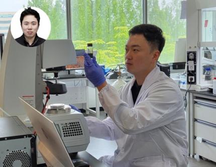
< Photo 1. (From left) Professor Steve Park of Materials Science and Engineering, Kyusoon Pak, Ph.D. Candidate (Army Major) >
Traditional military training often relies on standardized methods, which has limited the provision of optimized training tailored to individual combatants' characteristics or specific combat situations. To address this, our research team developed an e-textile platform, securing core technology that can reflect the unique traits of individual combatants and various combat scenarios. This technology has proven robust enough for battlefield use and is economical enough for widespread distribution to a large number of troops.
On June 25th, Professor Steve Park's research team at KAIST's Department of Materials Science and Engineering announced the development of a flexible, wearable electronic textile (E-textile) platform using an innovative technology that 'draws' electronic circuits directly onto fabric.
The wearable e-textile platform developed by the research team combines 3D printing technology with new materials engineering design to directly print flexible and highly durable sensors and electrodes onto textile substrates. This enables the collection of precise movement and human body data from individual combatants, which can then be used to propose customized training models.
Existing e-textile fabrication methods were often complex or limited in their ability to provide personalized customization. To overcome these challenges, the research team adopted an additive manufacturing technology called 'Direct Ink Writing (DIW)' 3D printing.
< Figure 1. Schematic diagram of e-textile manufactured with Direct Ink Writing (DIW) printing technology on various textiles, including combat uniforms >
This technology involves directly dispensing and printing special ink, which functions as sensors and electrodes, onto textile substrates in desired patterns. This allows for flexible implementation of various designs without the complex process of mask fabrication. This is expected to be an effective technology that can be easily supplied to hundreds of thousands of military personnel.
The core of this technology lies in the development of high-performance functional inks based on advanced materials engineering design. The research team combined styrene-butadiene-styrene (SBS) polymer, which provides flexibility, with multi-walled carbon nanotubes (MWCNT) for electrical conductivity. They developed a tensile/bending sensor ink that can stretch up to 102% and maintain stable performance even after 10,000 repetitive tests. This means that accurate data can be consistently obtained even during the strenuous movements of combatants.
< Figure 2. Measurement of human movement and breathing patterns using e-textile >
Furthermore, new material technology was applied to implement 'interconnect electrodes' that electrically connect the upper and lower layers of the fabric. The team developed an electrode ink combining silver (Ag) flakes with rigid polystyrene (PS) polymer, precisely controlling the impregnation level (how much the ink penetrates the fabric) to effectively connect both sides or multiple layers of the fabric. This secures the technology for producing multi-layered wearable electronic systems integrating sensors and electrodes.
< Figure 3. Experimental results of recognizing unknown objects after machine learning six objects using a smart glove >
The research team proved the platform's performance through actual human movement monitoring experiments. They printed the developed e-textile on major joint areas of clothing (shoulders, elbows, knees) and measured movements and posture changes during various exercises such as running, jumping jacks, and push-ups in real-time.
Additionally, they demonstrated the potential for applications such as monitoring breathing patterns using a smart mask and recognizing objects through machine learning and perceiving complex tactile information by printing multiple sensors and electrodes on gloves. These results show that the developed e-textile platform is effective in precisely understanding the movement dynamics of combatants.
This research is an important example demonstrating how cutting-edge new material technology can contribute to the advancement of the defense sector. Major Kyusoon Pak of the Army, who participated in this research, considered required objectives such as military applicability and economic feasibility for practical distribution from the research design stage.
< Figure 4. Experimental results showing that a multi-layered e-textile glove connected with interconnect electrodes can measure tensile/bending signals and pressure signals at a single point >
Major Pak stated, "Our military is currently facing both a crisis and an opportunity due to the decrease in military personnel resources caused by the demographic cliff and the advancement of science and technology. Also, respect for life in the battlefield is emerging as a significant issue. This research aims to secure original technology that can provide customized training according to military branch/duty and type of combat, thereby enhancing the combat power and ensuring the survivability of our soldiers."
He added, "I hope this research will be evaluated as a case that achieved both scientific contribution and military applicability."
This research, where Kyusoon Pak, Ph.D. Candidate (Army Major) from KAIST's Department of Materials Science and Engineering, participated as the first author and Professor Steve Park supervised, was published on May 27, 2025, in `npj Flexible Electronics (top 1.8% in JCR field)', an international academic journal in the electrical, electronic, and materials engineering fields.
* Paper Title: Fabrication of Multifunctional Wearable Interconnect E-textile Platform Using Direct Ink Writing (DIW) 3D Printing
* DOI: https://doi.org/10.1038/s41528-025-00414-7
This research was supported by the Ministry of Trade, Industry and Energy and the National Research Foundation of Korea.
2025.06.25 View 71
Military Combatants Usher in an Era of Personalized Training with New Materials
< Photo 1. (From left) Professor Steve Park of Materials Science and Engineering, Kyusoon Pak, Ph.D. Candidate (Army Major) >
Traditional military training often relies on standardized methods, which has limited the provision of optimized training tailored to individual combatants' characteristics or specific combat situations. To address this, our research team developed an e-textile platform, securing core technology that can reflect the unique traits of individual combatants and various combat scenarios. This technology has proven robust enough for battlefield use and is economical enough for widespread distribution to a large number of troops.
On June 25th, Professor Steve Park's research team at KAIST's Department of Materials Science and Engineering announced the development of a flexible, wearable electronic textile (E-textile) platform using an innovative technology that 'draws' electronic circuits directly onto fabric.
The wearable e-textile platform developed by the research team combines 3D printing technology with new materials engineering design to directly print flexible and highly durable sensors and electrodes onto textile substrates. This enables the collection of precise movement and human body data from individual combatants, which can then be used to propose customized training models.
Existing e-textile fabrication methods were often complex or limited in their ability to provide personalized customization. To overcome these challenges, the research team adopted an additive manufacturing technology called 'Direct Ink Writing (DIW)' 3D printing.
< Figure 1. Schematic diagram of e-textile manufactured with Direct Ink Writing (DIW) printing technology on various textiles, including combat uniforms >
This technology involves directly dispensing and printing special ink, which functions as sensors and electrodes, onto textile substrates in desired patterns. This allows for flexible implementation of various designs without the complex process of mask fabrication. This is expected to be an effective technology that can be easily supplied to hundreds of thousands of military personnel.
The core of this technology lies in the development of high-performance functional inks based on advanced materials engineering design. The research team combined styrene-butadiene-styrene (SBS) polymer, which provides flexibility, with multi-walled carbon nanotubes (MWCNT) for electrical conductivity. They developed a tensile/bending sensor ink that can stretch up to 102% and maintain stable performance even after 10,000 repetitive tests. This means that accurate data can be consistently obtained even during the strenuous movements of combatants.
< Figure 2. Measurement of human movement and breathing patterns using e-textile >
Furthermore, new material technology was applied to implement 'interconnect electrodes' that electrically connect the upper and lower layers of the fabric. The team developed an electrode ink combining silver (Ag) flakes with rigid polystyrene (PS) polymer, precisely controlling the impregnation level (how much the ink penetrates the fabric) to effectively connect both sides or multiple layers of the fabric. This secures the technology for producing multi-layered wearable electronic systems integrating sensors and electrodes.
< Figure 3. Experimental results of recognizing unknown objects after machine learning six objects using a smart glove >
The research team proved the platform's performance through actual human movement monitoring experiments. They printed the developed e-textile on major joint areas of clothing (shoulders, elbows, knees) and measured movements and posture changes during various exercises such as running, jumping jacks, and push-ups in real-time.
Additionally, they demonstrated the potential for applications such as monitoring breathing patterns using a smart mask and recognizing objects through machine learning and perceiving complex tactile information by printing multiple sensors and electrodes on gloves. These results show that the developed e-textile platform is effective in precisely understanding the movement dynamics of combatants.
This research is an important example demonstrating how cutting-edge new material technology can contribute to the advancement of the defense sector. Major Kyusoon Pak of the Army, who participated in this research, considered required objectives such as military applicability and economic feasibility for practical distribution from the research design stage.
< Figure 4. Experimental results showing that a multi-layered e-textile glove connected with interconnect electrodes can measure tensile/bending signals and pressure signals at a single point >
Major Pak stated, "Our military is currently facing both a crisis and an opportunity due to the decrease in military personnel resources caused by the demographic cliff and the advancement of science and technology. Also, respect for life in the battlefield is emerging as a significant issue. This research aims to secure original technology that can provide customized training according to military branch/duty and type of combat, thereby enhancing the combat power and ensuring the survivability of our soldiers."
He added, "I hope this research will be evaluated as a case that achieved both scientific contribution and military applicability."
This research, where Kyusoon Pak, Ph.D. Candidate (Army Major) from KAIST's Department of Materials Science and Engineering, participated as the first author and Professor Steve Park supervised, was published on May 27, 2025, in `npj Flexible Electronics (top 1.8% in JCR field)', an international academic journal in the electrical, electronic, and materials engineering fields.
* Paper Title: Fabrication of Multifunctional Wearable Interconnect E-textile Platform Using Direct Ink Writing (DIW) 3D Printing
* DOI: https://doi.org/10.1038/s41528-025-00414-7
This research was supported by the Ministry of Trade, Industry and Energy and the National Research Foundation of Korea.
2025.06.25 View 71 -
 KAIST Develops Customized Tactile Sensor That Can Detect Light Breath, Pressure and Sound
< Photo 1. (From left) Professor Inkyu Park of KAIST Department of Mechanical Engineering (ME), Dr. Jungrak Choi of ETRI, Ph.D. Candidate Donho Lee and M.S. Graduate Chankyu Han of KAIST ME >
When a robot grabs an object or a medical device detects a pulse, the tactile sensor is the technology that senses pressure like a fingertip. Existing sensors had disadvantages, such as slow responses or declining accuracy after repeated use, but Korean researchers have succeeded in developing a sensor that can quickly and accurately detect even light breath, pressure, and sound. This sensor can be used across a broad range — from everyday movements to medical diagnostics.
KAIST (represented by President Kwang Hyung Lee) announced on the 23rd of June that Professor Inkyu Park’s team from the Department of Mechanical Engineering, through a collaborative research project with the Electronics and Telecommunications Research Institute (ETRI, President Seung Chan Bang ) under the National Research Council of Science & Technology (NST, Chairman Young Sik Kim), has developed an innovative technology that overcomes the structural limitations of existing tactile sensors.
The core of this joint research is the implementation of a customized tactile sensor that simultaneously achieves flexibility, precision, and repeatable durability by applying Thermoformed 3D Electronics (T3DE).
< Figure 1. Comparative evaluation of soft elastomer–based 3D structure versus thermoforming-based 3D structure in terms of mechanical properties. >
In particular, soft elastomer-based sensors (rubber, silicone, etc. — materials that stretch and return to their original shape) have structural problems such as slow response times, high hysteresis*, and creep**, but this new platform operates precisely in diverse environments and overcomes these limitations.
*Hysteresis: A phenomenon where the previously applied force or change is retained like a “memory,” so that the same stimulus does not always produce the same result.
**Creep: The phenomenon where a material slowly deforms when a force is continuously applied.
T3DE sensors are manufactured by precisely forming electrodes on a 2D film, then thermoforming them into a 3D structure under heat and pressure. Specifically, the top electrodes and supporting pillar structures of the sensor are designed to allow the fine-tuning of the mechanical properties for different purposes. By adjusting microstructural parameters — such as the thickness, length, and number of support pillars — the sensor’s Young’s modulus* can be tuned across a broad range of 10 Pa to 1 MPa. This matches the stiffness of biological tissues like skin, muscle, and tendons, making them highly suitable as bio-interface sensors.
*Young’s modulus: An index representing a material's stiffness; this research can control this index to match various biological tissues.
The newly developed T3DE sensor uses air as a dielectric material to reduce power consumption and demonstrates outstanding performance in sensitivity, response time, thermal stability, and repeatable accuracy.
Experimental results showed that the sensor achieved △sensitivity of 5,884 kPa⁻¹, △response time of 0.1 ms (less than one-thousandth of a second), △hysteresis of less than 0.5%, and maintained a repeatable precision of 99.9% or higher even after 5,000 repeated measurements.
< Figure 2. Graphic Overview of thermoformed 3D electronics (T3DE) >
The research team also constructed a high-resolution 40×70 array, comprising a total of 2,800 densely packed sensors, to visualize the pressure distribution on the sole of the foot in real time during exercise and confirmed the possibility of using the sensor for wrist pulse measurement to assess vascular health. Furthermore, successful results were also achieved in sound-detection experiments at a level comparable to commercial acoustic sensors. In short, the sensor can precisely and quickly measure foot pressure, pulse, and sound, allowing it to be applied in areas such as sports, health, and sound sensing.
The T3DE technology was also applied to an augmented-reality(AR)-based surgical training system. By adjusting the stiffness of each sensor element to match that of biological tissues, the system provided real-time visual and tactile feedback according to the pressure applied during surgical incisions. It also offered real-time warnings if an incision was too deep or approached a risky area, making it a promising technology for enhancing immersion and accuracy in medical training.
KAIST Professor Inkyu Park stated, “Because this sensor can be precisely tuned from the design stage and operates reliably across diverse environments, it can be used not only in everyday life, but also in a variety of fields such as healthcare, rehabilitation, and virtual reality.”
The research was co-led as first authors by Dr. Jungrak Choi of ETRI, KAIST master’s student Chankyu Han, and Ph.D. candidate Donho Lee, under the overall guidance of Professor Inkyu Park. The research results were published in the May 2025 issue of ‘Science Advances’ and introduced to the global research community through the journal’s official SNS channels (Facebook, Twitter).
※ Thesis Title: Thermoforming 2D films into 3D electronics for high-performance, customizable tactile sensing
※ DOI: 10.1126/sciadv.adv0057
< Figure 3. The introduction of the study on the official SNS posting by Science Advances >
This research was supported by the Ministry of Trade, Industry and Energy, the National Research Foundation of Korea, and the Korea Institute for Advancement of Technology.
2025.06.23 View 224
KAIST Develops Customized Tactile Sensor That Can Detect Light Breath, Pressure and Sound
< Photo 1. (From left) Professor Inkyu Park of KAIST Department of Mechanical Engineering (ME), Dr. Jungrak Choi of ETRI, Ph.D. Candidate Donho Lee and M.S. Graduate Chankyu Han of KAIST ME >
When a robot grabs an object or a medical device detects a pulse, the tactile sensor is the technology that senses pressure like a fingertip. Existing sensors had disadvantages, such as slow responses or declining accuracy after repeated use, but Korean researchers have succeeded in developing a sensor that can quickly and accurately detect even light breath, pressure, and sound. This sensor can be used across a broad range — from everyday movements to medical diagnostics.
KAIST (represented by President Kwang Hyung Lee) announced on the 23rd of June that Professor Inkyu Park’s team from the Department of Mechanical Engineering, through a collaborative research project with the Electronics and Telecommunications Research Institute (ETRI, President Seung Chan Bang ) under the National Research Council of Science & Technology (NST, Chairman Young Sik Kim), has developed an innovative technology that overcomes the structural limitations of existing tactile sensors.
The core of this joint research is the implementation of a customized tactile sensor that simultaneously achieves flexibility, precision, and repeatable durability by applying Thermoformed 3D Electronics (T3DE).
< Figure 1. Comparative evaluation of soft elastomer–based 3D structure versus thermoforming-based 3D structure in terms of mechanical properties. >
In particular, soft elastomer-based sensors (rubber, silicone, etc. — materials that stretch and return to their original shape) have structural problems such as slow response times, high hysteresis*, and creep**, but this new platform operates precisely in diverse environments and overcomes these limitations.
*Hysteresis: A phenomenon where the previously applied force or change is retained like a “memory,” so that the same stimulus does not always produce the same result.
**Creep: The phenomenon where a material slowly deforms when a force is continuously applied.
T3DE sensors are manufactured by precisely forming electrodes on a 2D film, then thermoforming them into a 3D structure under heat and pressure. Specifically, the top electrodes and supporting pillar structures of the sensor are designed to allow the fine-tuning of the mechanical properties for different purposes. By adjusting microstructural parameters — such as the thickness, length, and number of support pillars — the sensor’s Young’s modulus* can be tuned across a broad range of 10 Pa to 1 MPa. This matches the stiffness of biological tissues like skin, muscle, and tendons, making them highly suitable as bio-interface sensors.
*Young’s modulus: An index representing a material's stiffness; this research can control this index to match various biological tissues.
The newly developed T3DE sensor uses air as a dielectric material to reduce power consumption and demonstrates outstanding performance in sensitivity, response time, thermal stability, and repeatable accuracy.
Experimental results showed that the sensor achieved △sensitivity of 5,884 kPa⁻¹, △response time of 0.1 ms (less than one-thousandth of a second), △hysteresis of less than 0.5%, and maintained a repeatable precision of 99.9% or higher even after 5,000 repeated measurements.
< Figure 2. Graphic Overview of thermoformed 3D electronics (T3DE) >
The research team also constructed a high-resolution 40×70 array, comprising a total of 2,800 densely packed sensors, to visualize the pressure distribution on the sole of the foot in real time during exercise and confirmed the possibility of using the sensor for wrist pulse measurement to assess vascular health. Furthermore, successful results were also achieved in sound-detection experiments at a level comparable to commercial acoustic sensors. In short, the sensor can precisely and quickly measure foot pressure, pulse, and sound, allowing it to be applied in areas such as sports, health, and sound sensing.
The T3DE technology was also applied to an augmented-reality(AR)-based surgical training system. By adjusting the stiffness of each sensor element to match that of biological tissues, the system provided real-time visual and tactile feedback according to the pressure applied during surgical incisions. It also offered real-time warnings if an incision was too deep or approached a risky area, making it a promising technology for enhancing immersion and accuracy in medical training.
KAIST Professor Inkyu Park stated, “Because this sensor can be precisely tuned from the design stage and operates reliably across diverse environments, it can be used not only in everyday life, but also in a variety of fields such as healthcare, rehabilitation, and virtual reality.”
The research was co-led as first authors by Dr. Jungrak Choi of ETRI, KAIST master’s student Chankyu Han, and Ph.D. candidate Donho Lee, under the overall guidance of Professor Inkyu Park. The research results were published in the May 2025 issue of ‘Science Advances’ and introduced to the global research community through the journal’s official SNS channels (Facebook, Twitter).
※ Thesis Title: Thermoforming 2D films into 3D electronics for high-performance, customizable tactile sensing
※ DOI: 10.1126/sciadv.adv0057
< Figure 3. The introduction of the study on the official SNS posting by Science Advances >
This research was supported by the Ministry of Trade, Industry and Energy, the National Research Foundation of Korea, and the Korea Institute for Advancement of Technology.
2025.06.23 View 224 -
 KAIST achieves quantum entanglement essential for quantum error correction
Quantum computing is a technology capable of solving complex problems that classical computers struggle with. To perform accurate computations, quantum computers must correct errors that arise during operations. However, generating the quantum entanglement necessary for quantum error correction has long been considered a major challenge.
< Photo 1. (From left) Students Young-Do Yoon and Chan Roh of the Master's and Doctoral Integrated Program of the Department of Physics poses with Professor Young-Sik Ra and Student Geunhee Gwak of the same program >
KAIST (represented by President Kwang Hyung Lee) announced on the 25th of February that a research team led by Professor Young-Sik Ra from the Department of Physics has successfully implemented a three-dimensional cluster quantum entangled state, a key component for quantum error correction, through experimental demonstration.
Measurement-based quantum computing is an emerging paradigm that implements quantum computations by measuring specially entangled cluster states. The core of this approach lies in the generation of these cluster quantum entangled states, with two-dimensional cluster states commonly used for universal quantum computing.
However, to advance towards fault-tolerant quantum computing, which can correct quantum errors occurring during computations, a more complex three-dimensional cluster state is required. While previous studies have reported the generation of two-dimensional cluster states, experimental implementation of the three-dimensional cluster states necessary for fault-tolerant quantum computing had remained elusive due to the extreme complexity of their entanglement structure.
< Figure 1. (a) Experimental schematic. A pulse laser with a wavelength of 800 nm is converted into a pulse laser with a wavelength of 400 nm through second harmonic generation, and this is incident on a nonlinear crystal (PPKTP) to generate multiple quantum entanglement sources. (b) Generation of a 3D cluster state through optical mode basis change >
The research team overcame this challenge by developing a technique to control femtosecond time-frequency modes, successfully generating a three-dimensional cluster quantum entangled state for the first time.
The team directed a femtosecond laser into a nonlinear crystal, simultaneously generating quantum light sources across multiple frequency modes. (A femtosecond laser is a device that emits ultrashort, high-intensity light pulses.) Using this approach, they successfully created a three-dimensional cluster quantum entangled state.
Professor Young-Sik Ra noted, “This study marks the first successful demonstration of a three-dimensional cluster quantum entangled state, which was previously difficult to achieve with existing technology. This breakthrough is expected to serve as a crucial stepping stone for future research in measurement-based and fault-tolerant quantum computing.”
< Figure 2. Results of 3D cluster state generation. (a) Nullifier measurement of the cluster state. (b) 3D cluster state reconstructed using quantum state tomography. (c) Confirmation of quantum entanglement characteristics of the 3D cluster state >
The study was published online in Nature Photonics on February 24, 2025. The first author is Chan Roh, a Ph.D. candidate in KAIST’s integrated master’s and doctoral program, with Geunhee Gwak and Youngdo Yoon contributing as co-authors. (Paper title: “Generation of Three-Dimensional Cluster Entangled State”, DOI: 10.1038/s41566-025-01631-2)
This research was supported by the National Research Foundation of Korea (Quantum Computing Technology Development Program, Mid-Career Researcher Support Program, and Quantum Simulator for Materials Innovation Program), the Institute for Information & Communications Technology Planning & Evaluation (Quantum Internet Core Technology Program, University ICT Research Center Support Program), and the U.S. Air Force Research Laboratory.
2025.02.25 View 2993
KAIST achieves quantum entanglement essential for quantum error correction
Quantum computing is a technology capable of solving complex problems that classical computers struggle with. To perform accurate computations, quantum computers must correct errors that arise during operations. However, generating the quantum entanglement necessary for quantum error correction has long been considered a major challenge.
< Photo 1. (From left) Students Young-Do Yoon and Chan Roh of the Master's and Doctoral Integrated Program of the Department of Physics poses with Professor Young-Sik Ra and Student Geunhee Gwak of the same program >
KAIST (represented by President Kwang Hyung Lee) announced on the 25th of February that a research team led by Professor Young-Sik Ra from the Department of Physics has successfully implemented a three-dimensional cluster quantum entangled state, a key component for quantum error correction, through experimental demonstration.
Measurement-based quantum computing is an emerging paradigm that implements quantum computations by measuring specially entangled cluster states. The core of this approach lies in the generation of these cluster quantum entangled states, with two-dimensional cluster states commonly used for universal quantum computing.
However, to advance towards fault-tolerant quantum computing, which can correct quantum errors occurring during computations, a more complex three-dimensional cluster state is required. While previous studies have reported the generation of two-dimensional cluster states, experimental implementation of the three-dimensional cluster states necessary for fault-tolerant quantum computing had remained elusive due to the extreme complexity of their entanglement structure.
< Figure 1. (a) Experimental schematic. A pulse laser with a wavelength of 800 nm is converted into a pulse laser with a wavelength of 400 nm through second harmonic generation, and this is incident on a nonlinear crystal (PPKTP) to generate multiple quantum entanglement sources. (b) Generation of a 3D cluster state through optical mode basis change >
The research team overcame this challenge by developing a technique to control femtosecond time-frequency modes, successfully generating a three-dimensional cluster quantum entangled state for the first time.
The team directed a femtosecond laser into a nonlinear crystal, simultaneously generating quantum light sources across multiple frequency modes. (A femtosecond laser is a device that emits ultrashort, high-intensity light pulses.) Using this approach, they successfully created a three-dimensional cluster quantum entangled state.
Professor Young-Sik Ra noted, “This study marks the first successful demonstration of a three-dimensional cluster quantum entangled state, which was previously difficult to achieve with existing technology. This breakthrough is expected to serve as a crucial stepping stone for future research in measurement-based and fault-tolerant quantum computing.”
< Figure 2. Results of 3D cluster state generation. (a) Nullifier measurement of the cluster state. (b) 3D cluster state reconstructed using quantum state tomography. (c) Confirmation of quantum entanglement characteristics of the 3D cluster state >
The study was published online in Nature Photonics on February 24, 2025. The first author is Chan Roh, a Ph.D. candidate in KAIST’s integrated master’s and doctoral program, with Geunhee Gwak and Youngdo Yoon contributing as co-authors. (Paper title: “Generation of Three-Dimensional Cluster Entangled State”, DOI: 10.1038/s41566-025-01631-2)
This research was supported by the National Research Foundation of Korea (Quantum Computing Technology Development Program, Mid-Career Researcher Support Program, and Quantum Simulator for Materials Innovation Program), the Institute for Information & Communications Technology Planning & Evaluation (Quantum Internet Core Technology Program, University ICT Research Center Support Program), and the U.S. Air Force Research Laboratory.
2025.02.25 View 2993 -
 KAIST Research Team Develops an AI Framework Capable of Overcoming the Strength-Ductility Dilemma in Additive-manufactured Titanium Alloys
<(From Left) Ph.D. Student Jaejung Park and Professor Seungchul Lee of KAIST Department of Mechanical Engineering and , Professor Hyoung Seop Kim of POSTECH, and M.S.–Ph.D. Integrated Program Student Jeong Ah Lee of POSTECH. >
The KAIST research team led by Professor Seungchul Lee from Department of Mechanical Engineering, in collaboration with Professor Hyoung Seop Kim’s team at POSTECH, successfully overcame the strength–ductility dilemma of Ti 6Al 4V alloy using artificial intelligence, enabling the production of high strength, high ductility metal products. The AI developed by the team accurately predicts mechanical properties based on various 3D printing process parameters while also providing uncertainty information, and it uses both to recommend process parameters that hold high promise for 3D printing.
Among various 3D printing technologies, laser powder bed fusion is an innovative method for manufacturing Ti-6Al-4V alloy, renowned for its high strength and bio-compatibility. However, this alloy made via 3D printing has traditionally faced challenges in simultaneously achieving high strength and high ductility. Although there have been attempts to address this issue by adjusting both the printing process parameters and heat treatment conditions, the vast number of possible combinations made it difficult to explore them all through experiments and simulations alone.
The active learning framework developed by the team quickly explores a wide range of 3D printing process parameters and heat treatment conditions to recommend those expected to improve both strength and ductility of the alloy. These recommendations are based on the AI model’s predictions of ultimate tensile strength and total elongation along with associated uncertainty information for each set of process parameters and heat treatment conditions. The recommended conditions are then validated by performing 3D printing and tensile tests to obtain the true mechanical property values. These new data are incorporated into further AI model training, and through iterative exploration, the optimal process parameters and heat treatment conditions for producing high-performance alloys were determined in only five iterations. With these optimized conditions, the 3D printed Ti-6Al-4V alloy achieved an ultimate tensile strength of 1190 MPa and a total elongation of 16.5%, successfully overcoming the strength–ductility dilemma.
Professor Seungchul Lee commented, “In this study, by optimizing the 3D printing process parameters and heat treatment conditions, we were able to develop a high-strength, high-ductility Ti-6Al-4V alloy with minimal experimentation trials. Compared to previous studies, we produced an alloy with a similar ultimate tensile strength but higher total elongation, as well as that with a similar elongation but greater ultimate tensile strength.” He added, “Furthermore, if our approach is applied not only to mechanical properties but also to other properties such as thermal conductivity and thermal expansion, we anticipate that it will enable efficient exploration of 3D printing process parameters and heat treatment conditions.”
This study was published in Nature Communications on January 22 (https://doi.org/10.1038/s41467-025-56267-1), and the research was supported by the National Research Foundation of Korea’s Nano & Material Technology Development Program and the Leading Research Center Program.
2025.02.21 View 4794
KAIST Research Team Develops an AI Framework Capable of Overcoming the Strength-Ductility Dilemma in Additive-manufactured Titanium Alloys
<(From Left) Ph.D. Student Jaejung Park and Professor Seungchul Lee of KAIST Department of Mechanical Engineering and , Professor Hyoung Seop Kim of POSTECH, and M.S.–Ph.D. Integrated Program Student Jeong Ah Lee of POSTECH. >
The KAIST research team led by Professor Seungchul Lee from Department of Mechanical Engineering, in collaboration with Professor Hyoung Seop Kim’s team at POSTECH, successfully overcame the strength–ductility dilemma of Ti 6Al 4V alloy using artificial intelligence, enabling the production of high strength, high ductility metal products. The AI developed by the team accurately predicts mechanical properties based on various 3D printing process parameters while also providing uncertainty information, and it uses both to recommend process parameters that hold high promise for 3D printing.
Among various 3D printing technologies, laser powder bed fusion is an innovative method for manufacturing Ti-6Al-4V alloy, renowned for its high strength and bio-compatibility. However, this alloy made via 3D printing has traditionally faced challenges in simultaneously achieving high strength and high ductility. Although there have been attempts to address this issue by adjusting both the printing process parameters and heat treatment conditions, the vast number of possible combinations made it difficult to explore them all through experiments and simulations alone.
The active learning framework developed by the team quickly explores a wide range of 3D printing process parameters and heat treatment conditions to recommend those expected to improve both strength and ductility of the alloy. These recommendations are based on the AI model’s predictions of ultimate tensile strength and total elongation along with associated uncertainty information for each set of process parameters and heat treatment conditions. The recommended conditions are then validated by performing 3D printing and tensile tests to obtain the true mechanical property values. These new data are incorporated into further AI model training, and through iterative exploration, the optimal process parameters and heat treatment conditions for producing high-performance alloys were determined in only five iterations. With these optimized conditions, the 3D printed Ti-6Al-4V alloy achieved an ultimate tensile strength of 1190 MPa and a total elongation of 16.5%, successfully overcoming the strength–ductility dilemma.
Professor Seungchul Lee commented, “In this study, by optimizing the 3D printing process parameters and heat treatment conditions, we were able to develop a high-strength, high-ductility Ti-6Al-4V alloy with minimal experimentation trials. Compared to previous studies, we produced an alloy with a similar ultimate tensile strength but higher total elongation, as well as that with a similar elongation but greater ultimate tensile strength.” He added, “Furthermore, if our approach is applied not only to mechanical properties but also to other properties such as thermal conductivity and thermal expansion, we anticipate that it will enable efficient exploration of 3D printing process parameters and heat treatment conditions.”
This study was published in Nature Communications on January 22 (https://doi.org/10.1038/s41467-025-56267-1), and the research was supported by the National Research Foundation of Korea’s Nano & Material Technology Development Program and the Leading Research Center Program.
2025.02.21 View 4794 -
 KAIST Secures Core Technology for Ultra-High-Resolution Image Sensors
A joint research team from Korea and the United States has developed next-generation, high-resolution image sensor technology with higher power efficiency and a smaller size compared to existing sensors. Notably, they have secured foundational technology for ultra-high-resolution shortwave infrared (SWIR) image sensors, an area currently dominated by Sony, paving the way for future market entry.
KAIST (represented by President Kwang Hyung Lee) announced on the 20th of November that a research team led by Professor SangHyeon Kim from the School of Electrical Engineering, in collaboration with Inha University and Yale University in the U.S., has developed an ultra-thin broadband photodiode (PD), marking a significant breakthrough in high-performance image sensor technology.
This research drastically improves the trade-off between the absorption layer thickness and quantum efficiency found in conventional photodiode technology. Specifically, it achieved high quantum efficiency of over 70% even in an absorption layer thinner than one micrometer (μm), reducing the thickness of the absorption layer by approximately 70% compared to existing technologies.
A thinner absorption layer simplifies pixel processing, allowing for higher resolution and smoother carrier diffusion, which is advantageous for light carrier acquisition while also reducing the cost. However, a fundamental issue with thinner absorption layers is the reduced absorption of long-wavelength light.
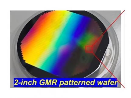
< Figure 1. Schematic diagram of the InGaAs photodiode image sensor integrated on the Guided-Mode Resonance (GMR) structure proposed in this study (left), a photograph of the fabricated wafer, and a scanning electron microscope (SEM) image of the periodic patterns (right) >
The research team introduced a guided-mode resonance (GMR) structure* that enables high-efficiency light absorption across a wide spectral range from 400 nanometers (nm) to 1,700 nanometers (nm). This wavelength range includes not only visible light but also light the SWIR region, making it valuable for various industrial applications.
*Guided-Mode Resonance (GMR) Structure: A concept used in electromagnetics, a phenomenon in which a specific (light) wave resonates (forming a strong electric/magnetic field) at a specific wavelength. Since energy is maximized under these conditions, it has been used to increase antenna or radar efficiency.
The improved performance in the SWIR region is expected to play a significant role in developing next-generation image sensors with increasingly high resolutions. The GMR structure, in particular, holds potential for further enhancing resolution and other performance metrics through hybrid integration and monolithic 3D integration with complementary metal-oxide-semiconductor (CMOS)-based readout integrated circuits (ROIC).
< Figure 2. Benchmark for state-of-the-art InGaAs-based SWIR pixels with simulated EQE lines as a function of TAL variation. Performance is maintained while reducing the absorption layer thickness from 2.1 micrometers or more to 1 micrometer or less while reducing it by 50% to 70% >
The research team has significantly enhanced international competitiveness in low-power devices and ultra-high-resolution imaging technology, opening up possibilities for applications in digital cameras, security systems, medical and industrial image sensors, as well as future ultra-high-resolution sensors for autonomous driving, aerospace, and satellite observation.
Professor Sang Hyun Kim, the lead researcher, commented, “This research demonstrates that significantly higher performance than existing technologies can be achieved even with ultra-thin absorption layers.”
< Figure 3. Top optical microscope image and cross-sectional scanning electron microscope image of the InGaAs photodiode image sensor fabricated on the GMR structure (left). Improved quantum efficiency performance of the ultra-thin image sensor (red) fabricated with the technology proposed in this study (right) >
The results of this research were published on 15th of November, in the prestigious international journal Light: Science & Applications (JCR 2.9%, IF=20.6), with Professor Dae-Myung Geum of Inha University (formerly a KAIST postdoctoral researcher) and Dr. Jinha Lim (currently a postdoctoral researcher at Yale University) as co-first authors. (Paper title: “Highly-efficient (>70%) and Wide-spectral (400 nm -1700 nm) sub-micron-thick InGaAs photodiodes for future high-resolution image sensors”)
This study was supported by the National Research Foundation of Korea.
2024.11.22 View 5348
KAIST Secures Core Technology for Ultra-High-Resolution Image Sensors
A joint research team from Korea and the United States has developed next-generation, high-resolution image sensor technology with higher power efficiency and a smaller size compared to existing sensors. Notably, they have secured foundational technology for ultra-high-resolution shortwave infrared (SWIR) image sensors, an area currently dominated by Sony, paving the way for future market entry.
KAIST (represented by President Kwang Hyung Lee) announced on the 20th of November that a research team led by Professor SangHyeon Kim from the School of Electrical Engineering, in collaboration with Inha University and Yale University in the U.S., has developed an ultra-thin broadband photodiode (PD), marking a significant breakthrough in high-performance image sensor technology.
This research drastically improves the trade-off between the absorption layer thickness and quantum efficiency found in conventional photodiode technology. Specifically, it achieved high quantum efficiency of over 70% even in an absorption layer thinner than one micrometer (μm), reducing the thickness of the absorption layer by approximately 70% compared to existing technologies.
A thinner absorption layer simplifies pixel processing, allowing for higher resolution and smoother carrier diffusion, which is advantageous for light carrier acquisition while also reducing the cost. However, a fundamental issue with thinner absorption layers is the reduced absorption of long-wavelength light.
< Figure 1. Schematic diagram of the InGaAs photodiode image sensor integrated on the Guided-Mode Resonance (GMR) structure proposed in this study (left), a photograph of the fabricated wafer, and a scanning electron microscope (SEM) image of the periodic patterns (right) >
The research team introduced a guided-mode resonance (GMR) structure* that enables high-efficiency light absorption across a wide spectral range from 400 nanometers (nm) to 1,700 nanometers (nm). This wavelength range includes not only visible light but also light the SWIR region, making it valuable for various industrial applications.
*Guided-Mode Resonance (GMR) Structure: A concept used in electromagnetics, a phenomenon in which a specific (light) wave resonates (forming a strong electric/magnetic field) at a specific wavelength. Since energy is maximized under these conditions, it has been used to increase antenna or radar efficiency.
The improved performance in the SWIR region is expected to play a significant role in developing next-generation image sensors with increasingly high resolutions. The GMR structure, in particular, holds potential for further enhancing resolution and other performance metrics through hybrid integration and monolithic 3D integration with complementary metal-oxide-semiconductor (CMOS)-based readout integrated circuits (ROIC).
< Figure 2. Benchmark for state-of-the-art InGaAs-based SWIR pixels with simulated EQE lines as a function of TAL variation. Performance is maintained while reducing the absorption layer thickness from 2.1 micrometers or more to 1 micrometer or less while reducing it by 50% to 70% >
The research team has significantly enhanced international competitiveness in low-power devices and ultra-high-resolution imaging technology, opening up possibilities for applications in digital cameras, security systems, medical and industrial image sensors, as well as future ultra-high-resolution sensors for autonomous driving, aerospace, and satellite observation.
Professor Sang Hyun Kim, the lead researcher, commented, “This research demonstrates that significantly higher performance than existing technologies can be achieved even with ultra-thin absorption layers.”
< Figure 3. Top optical microscope image and cross-sectional scanning electron microscope image of the InGaAs photodiode image sensor fabricated on the GMR structure (left). Improved quantum efficiency performance of the ultra-thin image sensor (red) fabricated with the technology proposed in this study (right) >
The results of this research were published on 15th of November, in the prestigious international journal Light: Science & Applications (JCR 2.9%, IF=20.6), with Professor Dae-Myung Geum of Inha University (formerly a KAIST postdoctoral researcher) and Dr. Jinha Lim (currently a postdoctoral researcher at Yale University) as co-first authors. (Paper title: “Highly-efficient (>70%) and Wide-spectral (400 nm -1700 nm) sub-micron-thick InGaAs photodiodes for future high-resolution image sensors”)
This study was supported by the National Research Foundation of Korea.
2024.11.22 View 5348 -
 A 20-year-old puzzle solved: KAIST research team reveals the 'three-dimensional vortex' of zero-dimensional ferroelectrics
Materials that can maintain a magnetized state by themselves without an external magnetic field (i.e., permanent magnets) are called ferromagnets. Ferroelectrics can be thought of as the electric counterpart to ferromagnets, as they maintain a polarized state without an external electric field. It is well-known that ferromagnets lose their magnetic properties when reduced to nano sizes below a certain threshold. What happens when ferroelectrics are similarly made extremely small in all directions (i.e., into a zero-dimensional structure such as nanoparticles) has been a topic of controversy for a long time.
< (From left) Professor Yongsoo Yang, the corresponding author, and Chaehwa Jeong, the first author studying in the integrated master’s and doctoral program, of the KAIST Department of Physics >
The research team led by Dr. Yongsoo Yang from the Department of Physics at KAIST has, for the first time, experimentally clarified the three-dimensional, vortex-shaped polarization distribution inside ferroelectric nanoparticles through international collaborative research with POSTECH, SNU, KBSI, LBNL and University of Arkansas.
About 20 years ago, Prof. Laurent Bellaiche (currently at University of Arkansas) and his colleagues theoretically predicted that a unique form of polarization distribution, arranged in a toroidal vortex shape, could occur inside ferroelectric nanodots. They also suggested that if this vortex distribution could be properly controlled, it could be applied to ultra-high-density memory devices with capacities over 10,000 times greater than existing ones. However, experimental clarification had not been achieved due to the difficulty of measuring the three-dimensional polarization distribution within ferroelectric nanostructures.
The research team at KAIST successfully solved this 20-year-old challenge by implementing a technique called atomic electron tomography. This technique works by acquiring atomic-resolution transmission electron microscope images of the nanomaterials from multiple tilt angles, and then reconstructing them back into three-dimensional structures using advanced reconstruction algorithms. Electron tomography can be understood as essentially the same method with the CT scans used in hospitals to view internal organs in three dimensions; the KAIST team adapted it uniquely for nanomaterials, utilizing an electron microscope at the single-atom level.
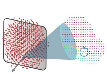
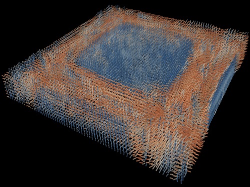
< Figure 1. Three-dimensional polarization distribution of BaTiO3 nanoparticles revealed by atomic electron tomography. >(Left) Schematic of the electron tomography technique, which involves acquiring transmission electron microscope images at multiple tilt angles and reconstructing them into 3D atomic structures.(Center) Experimentally determined three-dimensional polarization distribution inside a BaTiO3 nanoparticle via atomic electron tomography. A vortex-like structure is clearly visible near the bottom (blue dot).(Right) A two-dimensional cross-section of the polarization distribution, thinly sliced at the center of the vortex, with the color and arrows together indicating the direction of the polarization. A distinct vortex structure can be observed.
Using atomic electron tomography, the team completely measured the positions of cation atoms inside barium titanate (BaTiO3) nanoparticles, a well-known ferroelectric material, in three dimensions. From the precisely determined 3D atomic arrangements, they were able to further calculate the internal three-dimensional polarization distribution at the single-atom level. The analysis of the polarization distribution revealed, for the first time experimentally, that topological polarization orderings including vortices, anti-vortices, skyrmions, and a Bloch point occur inside the 0-dimensional ferroelectrics, as theoretically predicted 20 years ago. Furthermore, it was also found that the number of internal vortices can be controlled depending on their sizes.
Prof. Sergey Prosandeev and Prof. Bellaiche (who proposed with other co-workers the polar vortex ordering theoretically 20 years ago), joined this collaboration and further proved that the vortex distribution results obtained from experiments are consistent with theoretical calculations.
By controlling the number and orientation of these polarization distributions, it is expected that this can be utilized into next-generation high-density memory device that can store more than 10,000 times the amount of information in the same-sized device compared to existing ones.
Dr. Yang, who led the research, explained the significance of the results: “This result suggests that controlling the size and shape of ferroelectrics alone, without needing to tune the substrate or surrounding environmental effects such as epitaxial strain, can manipulate ferroelectric vortices or other topological orderings at the nano-scale. Further research could then be applied to the development of next-generation ultra-high-density memory.”
This research, with Chaehwa Jeong from the Department of Physics at KAIST as the first author, was published online in Nature Communications on May 8th (Title: Revealing the Three-Dimensional Arrangement of Polar Topology in Nanoparticles).
The study was mainly supported by the National Research Foundation of Korea (NRF) Grants funded by the Korean Government (MSIT).
2024.05.31 View 7516
A 20-year-old puzzle solved: KAIST research team reveals the 'three-dimensional vortex' of zero-dimensional ferroelectrics
Materials that can maintain a magnetized state by themselves without an external magnetic field (i.e., permanent magnets) are called ferromagnets. Ferroelectrics can be thought of as the electric counterpart to ferromagnets, as they maintain a polarized state without an external electric field. It is well-known that ferromagnets lose their magnetic properties when reduced to nano sizes below a certain threshold. What happens when ferroelectrics are similarly made extremely small in all directions (i.e., into a zero-dimensional structure such as nanoparticles) has been a topic of controversy for a long time.
< (From left) Professor Yongsoo Yang, the corresponding author, and Chaehwa Jeong, the first author studying in the integrated master’s and doctoral program, of the KAIST Department of Physics >
The research team led by Dr. Yongsoo Yang from the Department of Physics at KAIST has, for the first time, experimentally clarified the three-dimensional, vortex-shaped polarization distribution inside ferroelectric nanoparticles through international collaborative research with POSTECH, SNU, KBSI, LBNL and University of Arkansas.
About 20 years ago, Prof. Laurent Bellaiche (currently at University of Arkansas) and his colleagues theoretically predicted that a unique form of polarization distribution, arranged in a toroidal vortex shape, could occur inside ferroelectric nanodots. They also suggested that if this vortex distribution could be properly controlled, it could be applied to ultra-high-density memory devices with capacities over 10,000 times greater than existing ones. However, experimental clarification had not been achieved due to the difficulty of measuring the three-dimensional polarization distribution within ferroelectric nanostructures.
The research team at KAIST successfully solved this 20-year-old challenge by implementing a technique called atomic electron tomography. This technique works by acquiring atomic-resolution transmission electron microscope images of the nanomaterials from multiple tilt angles, and then reconstructing them back into three-dimensional structures using advanced reconstruction algorithms. Electron tomography can be understood as essentially the same method with the CT scans used in hospitals to view internal organs in three dimensions; the KAIST team adapted it uniquely for nanomaterials, utilizing an electron microscope at the single-atom level.
< Figure 1. Three-dimensional polarization distribution of BaTiO3 nanoparticles revealed by atomic electron tomography. >(Left) Schematic of the electron tomography technique, which involves acquiring transmission electron microscope images at multiple tilt angles and reconstructing them into 3D atomic structures.(Center) Experimentally determined three-dimensional polarization distribution inside a BaTiO3 nanoparticle via atomic electron tomography. A vortex-like structure is clearly visible near the bottom (blue dot).(Right) A two-dimensional cross-section of the polarization distribution, thinly sliced at the center of the vortex, with the color and arrows together indicating the direction of the polarization. A distinct vortex structure can be observed.
Using atomic electron tomography, the team completely measured the positions of cation atoms inside barium titanate (BaTiO3) nanoparticles, a well-known ferroelectric material, in three dimensions. From the precisely determined 3D atomic arrangements, they were able to further calculate the internal three-dimensional polarization distribution at the single-atom level. The analysis of the polarization distribution revealed, for the first time experimentally, that topological polarization orderings including vortices, anti-vortices, skyrmions, and a Bloch point occur inside the 0-dimensional ferroelectrics, as theoretically predicted 20 years ago. Furthermore, it was also found that the number of internal vortices can be controlled depending on their sizes.
Prof. Sergey Prosandeev and Prof. Bellaiche (who proposed with other co-workers the polar vortex ordering theoretically 20 years ago), joined this collaboration and further proved that the vortex distribution results obtained from experiments are consistent with theoretical calculations.
By controlling the number and orientation of these polarization distributions, it is expected that this can be utilized into next-generation high-density memory device that can store more than 10,000 times the amount of information in the same-sized device compared to existing ones.
Dr. Yang, who led the research, explained the significance of the results: “This result suggests that controlling the size and shape of ferroelectrics alone, without needing to tune the substrate or surrounding environmental effects such as epitaxial strain, can manipulate ferroelectric vortices or other topological orderings at the nano-scale. Further research could then be applied to the development of next-generation ultra-high-density memory.”
This research, with Chaehwa Jeong from the Department of Physics at KAIST as the first author, was published online in Nature Communications on May 8th (Title: Revealing the Three-Dimensional Arrangement of Polar Topology in Nanoparticles).
The study was mainly supported by the National Research Foundation of Korea (NRF) Grants funded by the Korean Government (MSIT).
2024.05.31 View 7516 -
 KAIST builds a high-resolution 3D holographic sensor using a single mask
Holographic cameras can provide more realistic images than ordinary cameras thanks to their ability to acquire 3D information about objects. However, existing holographic cameras use interferometers that measure the wavelength and refraction of light through the interference of light waves, which makes them complex and sensitive to their surrounding environment.
On August 23, a KAIST research team led by Professor YongKeun Park from the Department of Physics announced a new leap forward in 3D holographic imaging sensor technology.
The team proposed an innovative holographic camera technology that does not use complex interferometry. Instead, it uses a mask to precisely measure the phase information of light and reconstruct the 3D information of an object with higher accuracy.
< Figure 1. Structure and principle of the proposed holographic camera. The amplitude and phase information of light scattered from a holographic camera can be measured. >
The team used a mask that fulfills certain mathematical conditions and incorporated it into an ordinary camera, and the light scattered from a laser is measured through the mask and analyzed using a computer. This does not require a complex interferometer and allows the phase information of light to be collected through a simplified optical system. With this technique, the mask that is placed between the two lenses and behind an object plays an important role. The mask selectively filters specific parts of light,, and the intensity of the light passing through the lens can be measured using an ordinary commercial camera. This technique combines the image data received from the camera with the unique pattern received from the mask and reconstructs an object’s precise 3D information using an algorithm.
This method allows a high-resolution 3D image of an object to be captured in any position. In practical situations, one can construct a laser-based holographic 3D image sensor by adding a mask with a simple design to a general image sensor. This makes the design and construction of the optical system much easier. In particular, this novel technology can capture high-resolution holographic images of objects moving at high speeds, which widens its potential field of application.
< Figure 2. A moving doll captured by a conventional camera and the proposed holographic camera. When taking a picture without focusing on the object, only a blurred image of the doll can be obtained from a general camera, but the proposed holographic camera can restore the blurred image of the doll into a clear image. >
The results of this study, conducted by Dr. Jeonghun Oh from the KAIST Department of Physics as the first author, were published in Nature Communications on August 12 under the title, "Non-interferometric stand-alone single-shot holographic camera using reciprocal diffractive imaging".
Dr. Oh said, “The holographic camera module we are suggesting can be built by adding a filter to an ordinary camera, which would allow even non-experts to handle it easily in everyday life if it were to be commercialized.” He added, “In particular, it is a promising candidate with the potential to replace existing remote sensing technologies.”
This research was supported by the National Research Foundation’s Leader Research Project, the Korean Ministry of Science and ICT’s Core Hologram Technology Support Project, and the Nano and Material Technology Development Project.
2023.09.05 View 8759
KAIST builds a high-resolution 3D holographic sensor using a single mask
Holographic cameras can provide more realistic images than ordinary cameras thanks to their ability to acquire 3D information about objects. However, existing holographic cameras use interferometers that measure the wavelength and refraction of light through the interference of light waves, which makes them complex and sensitive to their surrounding environment.
On August 23, a KAIST research team led by Professor YongKeun Park from the Department of Physics announced a new leap forward in 3D holographic imaging sensor technology.
The team proposed an innovative holographic camera technology that does not use complex interferometry. Instead, it uses a mask to precisely measure the phase information of light and reconstruct the 3D information of an object with higher accuracy.
< Figure 1. Structure and principle of the proposed holographic camera. The amplitude and phase information of light scattered from a holographic camera can be measured. >
The team used a mask that fulfills certain mathematical conditions and incorporated it into an ordinary camera, and the light scattered from a laser is measured through the mask and analyzed using a computer. This does not require a complex interferometer and allows the phase information of light to be collected through a simplified optical system. With this technique, the mask that is placed between the two lenses and behind an object plays an important role. The mask selectively filters specific parts of light,, and the intensity of the light passing through the lens can be measured using an ordinary commercial camera. This technique combines the image data received from the camera with the unique pattern received from the mask and reconstructs an object’s precise 3D information using an algorithm.
This method allows a high-resolution 3D image of an object to be captured in any position. In practical situations, one can construct a laser-based holographic 3D image sensor by adding a mask with a simple design to a general image sensor. This makes the design and construction of the optical system much easier. In particular, this novel technology can capture high-resolution holographic images of objects moving at high speeds, which widens its potential field of application.
< Figure 2. A moving doll captured by a conventional camera and the proposed holographic camera. When taking a picture without focusing on the object, only a blurred image of the doll can be obtained from a general camera, but the proposed holographic camera can restore the blurred image of the doll into a clear image. >
The results of this study, conducted by Dr. Jeonghun Oh from the KAIST Department of Physics as the first author, were published in Nature Communications on August 12 under the title, "Non-interferometric stand-alone single-shot holographic camera using reciprocal diffractive imaging".
Dr. Oh said, “The holographic camera module we are suggesting can be built by adding a filter to an ordinary camera, which would allow even non-experts to handle it easily in everyday life if it were to be commercialized.” He added, “In particular, it is a promising candidate with the potential to replace existing remote sensing technologies.”
This research was supported by the National Research Foundation’s Leader Research Project, the Korean Ministry of Science and ICT’s Core Hologram Technology Support Project, and the Nano and Material Technology Development Project.
2023.09.05 View 8759 -
 Tomographic Measurement of Dielectric Tensors
Dielectric tensor tomography allows the direct measurement of the 3D dielectric tensors of optically anisotropic structures
A research team reported the direct measurement of dielectric tensors of anisotropic structures including the spatial variations of principal refractive indices and directors. The group also demonstrated quantitative tomographic measurements of various nematic liquid-crystal structures and their fast 3D nonequilibrium dynamics using a 3D label-free tomographic method. The method was described in Nature Materials.
Light-matter interactions are described by the dielectric tensor. Despite their importance in basic science and applications, it has not been possible to measure 3D dielectric tensors directly. The main challenge was due to the vectorial nature of light scattering from a 3D anisotropic structure. Previous approaches only addressed 3D anisotropic information indirectly and were limited to two-dimensional, qualitative, strict sample conditions or assumptions.
The research team developed a method enabling the tomographic reconstruction of 3D dielectric tensors without any preparation or assumptions. A sample is illuminated with a laser beam with various angles and circularly polarization states. Then, the light fields scattered from a sample are holographically measured and converted into vectorial diffraction components. Finally, by inversely solving a vectorial wave equation, the 3D dielectric tensor is reconstructed.
Professor YongKeun Park said, “There were a greater number of unknowns in direct measuring than with the conventional approach. We applied our approach to measure additional holographic images by slightly tilting the incident angle.”
He said that the slightly tilted illumination provides an additional orthogonal polarization, which makes the underdetermined problem become the determined problem. “Although scattered fields are dependent on the illumination angle, the Fourier differentiation theorem enables the extraction of the same dielectric tensor for the slightly tilted illumination,” Professor Park added.
His team’s method was validated by reconstructing well-known liquid crystal (LC) structures, including the twisted nematic, hybrid aligned nematic, radial, and bipolar configurations. Furthermore, the research team demonstrated the experimental measurements of the non-equilibrium dynamics of annihilating, nucleating, and merging LC droplets, and the LC polymer network with repeating 3D topological defects.
“This is the first experimental measurement of non-equilibrium dynamics and 3D topological defects in LC structures in a label-free manner. Our method enables the exploration of inaccessible nematic structures and interactions in non-equilibrium dynamics,” first author Dr. Seungwoo Shin explained.
-PublicationSeungwoo Shin, Jonghee Eun, Sang Seok Lee, Changjae Lee, Herve Hugonnet, Dong Ki Yoon, Shin-Hyun Kim, Jongwoo Jeong, YongKeun Park, “Tomographic Measurement ofDielectric Tensors at Optical Frequency,” Nature Materials March 02, 2022 (https://doi.org/10/1038/s41563-022-01202-8)
-ProfileProfessor YongKeun ParkBiomedical Optics Laboratory (http://bmol.kaist.ac.kr)Department of PhysicsCollege of Natural SciencesKAIST
2022.03.22 View 9363
Tomographic Measurement of Dielectric Tensors
Dielectric tensor tomography allows the direct measurement of the 3D dielectric tensors of optically anisotropic structures
A research team reported the direct measurement of dielectric tensors of anisotropic structures including the spatial variations of principal refractive indices and directors. The group also demonstrated quantitative tomographic measurements of various nematic liquid-crystal structures and their fast 3D nonequilibrium dynamics using a 3D label-free tomographic method. The method was described in Nature Materials.
Light-matter interactions are described by the dielectric tensor. Despite their importance in basic science and applications, it has not been possible to measure 3D dielectric tensors directly. The main challenge was due to the vectorial nature of light scattering from a 3D anisotropic structure. Previous approaches only addressed 3D anisotropic information indirectly and were limited to two-dimensional, qualitative, strict sample conditions or assumptions.
The research team developed a method enabling the tomographic reconstruction of 3D dielectric tensors without any preparation or assumptions. A sample is illuminated with a laser beam with various angles and circularly polarization states. Then, the light fields scattered from a sample are holographically measured and converted into vectorial diffraction components. Finally, by inversely solving a vectorial wave equation, the 3D dielectric tensor is reconstructed.
Professor YongKeun Park said, “There were a greater number of unknowns in direct measuring than with the conventional approach. We applied our approach to measure additional holographic images by slightly tilting the incident angle.”
He said that the slightly tilted illumination provides an additional orthogonal polarization, which makes the underdetermined problem become the determined problem. “Although scattered fields are dependent on the illumination angle, the Fourier differentiation theorem enables the extraction of the same dielectric tensor for the slightly tilted illumination,” Professor Park added.
His team’s method was validated by reconstructing well-known liquid crystal (LC) structures, including the twisted nematic, hybrid aligned nematic, radial, and bipolar configurations. Furthermore, the research team demonstrated the experimental measurements of the non-equilibrium dynamics of annihilating, nucleating, and merging LC droplets, and the LC polymer network with repeating 3D topological defects.
“This is the first experimental measurement of non-equilibrium dynamics and 3D topological defects in LC structures in a label-free manner. Our method enables the exploration of inaccessible nematic structures and interactions in non-equilibrium dynamics,” first author Dr. Seungwoo Shin explained.
-PublicationSeungwoo Shin, Jonghee Eun, Sang Seok Lee, Changjae Lee, Herve Hugonnet, Dong Ki Yoon, Shin-Hyun Kim, Jongwoo Jeong, YongKeun Park, “Tomographic Measurement ofDielectric Tensors at Optical Frequency,” Nature Materials March 02, 2022 (https://doi.org/10/1038/s41563-022-01202-8)
-ProfileProfessor YongKeun ParkBiomedical Optics Laboratory (http://bmol.kaist.ac.kr)Department of PhysicsCollege of Natural SciencesKAIST
2022.03.22 View 9363 -
 AI Light-Field Camera Reads 3D Facial Expressions
Machine-learned, light-field camera reads facial expressions from high-contrast illumination invariant 3D facial images
A joint research team led by Professors Ki-Hun Jeong and Doheon Lee from the KAIST Department of Bio and Brain Engineering reported the development of a technique for facial expression detection by merging near-infrared light-field camera techniques with artificial intelligence (AI) technology.
Unlike a conventional camera, the light-field camera contains micro-lens arrays in front of the image sensor, which makes the camera small enough to fit into a smart phone, while allowing it to acquire the spatial and directional information of the light with a single shot. The technique has received attention as it can reconstruct images in a variety of ways including multi-views, refocusing, and 3D image acquisition, giving rise to many potential applications.
However, the optical crosstalk between shadows caused by external light sources in the environment and the micro-lens has limited existing light-field cameras from being able to provide accurate image contrast and 3D reconstruction.
The joint research team applied a vertical-cavity surface-emitting laser (VCSEL) in the near-IR range to stabilize the accuracy of 3D image reconstruction that previously depended on environmental light. When an external light source is shone on a face at 0-, 30-, and 60-degree angles, the light field camera reduces 54% of image reconstruction errors. Additionally, by inserting a light-absorbing layer for visible and near-IR wavelengths between the micro-lens arrays, the team could minimize optical crosstalk while increasing the image contrast by 2.1 times.
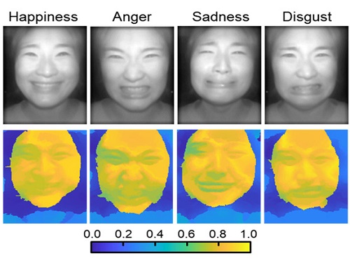
Through this technique, the team could overcome the limitations of existing light-field cameras and was able to develop their NIR-based light-field camera (NIR-LFC), optimized for the 3D image reconstruction of facial expressions. Using the NIR-LFC, the team acquired high-quality 3D reconstruction images of facial expressions expressing various emotions regardless of the lighting conditions of the surrounding environment.
The facial expressions in the acquired 3D images were distinguished through machine learning with an average of 85% accuracy – a statistically significant figure compared to when 2D images were used. Furthermore, by calculating the interdependency of distance information that varies with facial expression in 3D images, the team could identify the information a light-field camera utilizes to distinguish human expressions.
Professor Ki-Hun Jeong said, “The sub-miniature light-field camera developed by the research team has the potential to become the new platform to quantitatively analyze the facial expressions and emotions of humans.” To highlight the significance of this research, he added, “It could be applied in various fields including mobile healthcare, field diagnosis, social cognition, and human-machine interactions.”
This research was published in Advanced Intelligent Systems online on December 16, under the title, “Machine-Learned Light-field Camera that Reads Facial Expression from High-Contrast and Illumination Invariant 3D Facial Images.” This research was funded by the Ministry of Science and ICT and the Ministry of Trade, Industry and Energy.
-Publication“Machine-learned light-field camera that reads fascial expression from high-contrast and illumination invariant 3D facial images,” Sang-In Bae, Sangyeon Lee, Jae-Myeong Kwon, Hyun-Kyung Kim. Kyung-Won Jang, Doheon Lee, Ki-Hun Jeong, Advanced Intelligent Systems, December 16, 2021 (doi.org/10.1002/aisy.202100182)
ProfileProfessor Ki-Hun JeongBiophotonic LaboratoryDepartment of Bio and Brain EngineeringKAIST
Professor Doheon LeeDepartment of Bio and Brain EngineeringKAIST
2022.01.21 View 13708
AI Light-Field Camera Reads 3D Facial Expressions
Machine-learned, light-field camera reads facial expressions from high-contrast illumination invariant 3D facial images
A joint research team led by Professors Ki-Hun Jeong and Doheon Lee from the KAIST Department of Bio and Brain Engineering reported the development of a technique for facial expression detection by merging near-infrared light-field camera techniques with artificial intelligence (AI) technology.
Unlike a conventional camera, the light-field camera contains micro-lens arrays in front of the image sensor, which makes the camera small enough to fit into a smart phone, while allowing it to acquire the spatial and directional information of the light with a single shot. The technique has received attention as it can reconstruct images in a variety of ways including multi-views, refocusing, and 3D image acquisition, giving rise to many potential applications.
However, the optical crosstalk between shadows caused by external light sources in the environment and the micro-lens has limited existing light-field cameras from being able to provide accurate image contrast and 3D reconstruction.
The joint research team applied a vertical-cavity surface-emitting laser (VCSEL) in the near-IR range to stabilize the accuracy of 3D image reconstruction that previously depended on environmental light. When an external light source is shone on a face at 0-, 30-, and 60-degree angles, the light field camera reduces 54% of image reconstruction errors. Additionally, by inserting a light-absorbing layer for visible and near-IR wavelengths between the micro-lens arrays, the team could minimize optical crosstalk while increasing the image contrast by 2.1 times.
Through this technique, the team could overcome the limitations of existing light-field cameras and was able to develop their NIR-based light-field camera (NIR-LFC), optimized for the 3D image reconstruction of facial expressions. Using the NIR-LFC, the team acquired high-quality 3D reconstruction images of facial expressions expressing various emotions regardless of the lighting conditions of the surrounding environment.
The facial expressions in the acquired 3D images were distinguished through machine learning with an average of 85% accuracy – a statistically significant figure compared to when 2D images were used. Furthermore, by calculating the interdependency of distance information that varies with facial expression in 3D images, the team could identify the information a light-field camera utilizes to distinguish human expressions.
Professor Ki-Hun Jeong said, “The sub-miniature light-field camera developed by the research team has the potential to become the new platform to quantitatively analyze the facial expressions and emotions of humans.” To highlight the significance of this research, he added, “It could be applied in various fields including mobile healthcare, field diagnosis, social cognition, and human-machine interactions.”
This research was published in Advanced Intelligent Systems online on December 16, under the title, “Machine-Learned Light-field Camera that Reads Facial Expression from High-Contrast and Illumination Invariant 3D Facial Images.” This research was funded by the Ministry of Science and ICT and the Ministry of Trade, Industry and Energy.
-Publication“Machine-learned light-field camera that reads fascial expression from high-contrast and illumination invariant 3D facial images,” Sang-In Bae, Sangyeon Lee, Jae-Myeong Kwon, Hyun-Kyung Kim. Kyung-Won Jang, Doheon Lee, Ki-Hun Jeong, Advanced Intelligent Systems, December 16, 2021 (doi.org/10.1002/aisy.202100182)
ProfileProfessor Ki-Hun JeongBiophotonic LaboratoryDepartment of Bio and Brain EngineeringKAIST
Professor Doheon LeeDepartment of Bio and Brain EngineeringKAIST
2022.01.21 View 13708 -
 3D Visualization and Quantification of Bioplastic PHA in a Living Bacterial Cell
3D holographic microscopy leads to in-depth analysis of bacterial cells accumulating the bacterial bioplastic, polyhydroxyalkanoate (PHA)
A research team at KAIST has observed how bioplastic granule is being accumulated in living bacteria cells through 3D holographic microscopy. Their 3D imaging and quantitative analysis of the bioplastic ‘polyhydroxyalkanoate’ (PHA) via optical diffraction tomography provides insights into biosynthesizing sustainable substitutes for petroleum-based plastics.
The bio-degradable polyester polyhydroxyalkanoate (PHA) is being touted as an eco-friendly bioplastic to replace existing synthetic plastics. While carrying similar properties to general-purpose plastics such as polyethylene and polypropylene, PHA can be used in various industrial applications such as container packaging and disposable products.
PHA is synthesized by numerous bacteria as an energy and carbon storage material under unbalanced growth conditions in the presence of excess carbon sources. PHA exists in the form of insoluble granules in the cytoplasm. Previous studies on investigating in vivo PHA granules have been performed by using fluorescence microscopy, transmission electron microscopy (TEM), and electron cryotomography.
These techniques have generally relied on the statistical analysis of multiple 2D snapshots of fixed cells or the short-time monitoring of the cells. For the TEM analysis, cells need to be fixed and sectioned, and thus the investigation of living cells was not possible. Fluorescence-based techniques require fluorescence labeling or dye staining. Thus, indirect imaging with the use of reporter proteins cannot show the native state of PHAs or cells, and invasive exogenous dyes can affect the physiology and viability of the cells. Therefore, it was difficult to fully understand the formation of PHA granules in cells due to the technical limitations, and thus several mechanism models based on the observations have been only proposed.
The team of metabolic engineering researchers led by Distinguished Professor Sang Yup Lee and Physics Professor YongKeun Park, who established the startup Tomocube with his 3D holographic microscopy, reported the results of 3D quantitative label-free analysis of PHA granules in individual live bacterial cells by measuring the refractive index distributions using optical diffraction tomography. The formation and growth of PHA granules in the cells of Cupriavidus necator, the most-studied native PHA (specifically, poly(3-hydroxybutyrate), also known as PHB) producer, and recombinant Escherichia coli harboring C. necator PHB biosynthesis pathway were comparatively examined.
From the reconstructed 3D refractive index distribution of the cells, the team succeeded in the 3D visualization and quantitative analysis of cells and intracellular PHA granules at a single-cell level. In particular, the team newly presented the concept of “in vivo PHA granule density.” Through the statistical analysis of hundreds of single cells accumulating PHA granules, the distinctive differences of density and localization of PHA granules in the two micro-organisms were found. Furthermore, the team identified the key protein that plays a major role in making the difference that enabled the characteristics of PHA granules in the recombinant E. coli to become similar to those of C. necator.
The research team also presented 3D time-lapse movies showing the actual processes of PHA granule formation combined with cell growth and division. Movies showing the living cells synthesizing and accumulating PHA granules in their native state had never been reported before.
Professor Lee said, “This study provides insights into the morphological and physical characteristics of in vivo PHA as well as the unique mechanisms of PHA granule formation that undergo the phase transition from soluble monomers into the insoluble polymer, followed by granule formation. Through this study, a deeper understanding of PHA granule formation within the bacterial cells is now possible, which has great significance in that a convergence study of biology and physics was achieved. This study will help develop various bioplastics production processes in the future.”
This work was supported by the Technology Development Program to Solve Climate Changes on Systems Metabolic Engineering for Biorefineries (Grants NRF-2012M1A2A2026556 and NRF-2012M1A2A2026557) and the Bio & Medical Technology Development Program (Grant No. 2021M3A9I4022740) from the Ministry of Science and ICT (MSIT) through the National Research Foundation (NRF) of Korea to S.Y.L. This work was also supported by the KAIST Cross-Generation Collaborative Laboratory project.
-PublicationSo Young Choi, Jeonghun Oh, JaeHwang Jung, YongKeun Park, and Sang Yup Lee. Three-dimensional label-free visualization and quantification of polyhydroxyalkanoates in individualbacterial cell in its native state. PNAS(https://doi.org./10.1073/pnas.2103956118)
-ProfileDistinguished Professor Sang Yup LeeMetabolic Engineering and Synthetic Biologyhttp://mbel.kaist.ac.kr/
Department of Chemical and Biomolecular Engineering KAIST
Endowed Chair Professor YongKeun ParkBiomedical Optics Laboratoryhttps://bmokaist.wordpress.com/
Department of PhysicsKAIST
2021.07.28 View 15020
3D Visualization and Quantification of Bioplastic PHA in a Living Bacterial Cell
3D holographic microscopy leads to in-depth analysis of bacterial cells accumulating the bacterial bioplastic, polyhydroxyalkanoate (PHA)
A research team at KAIST has observed how bioplastic granule is being accumulated in living bacteria cells through 3D holographic microscopy. Their 3D imaging and quantitative analysis of the bioplastic ‘polyhydroxyalkanoate’ (PHA) via optical diffraction tomography provides insights into biosynthesizing sustainable substitutes for petroleum-based plastics.
The bio-degradable polyester polyhydroxyalkanoate (PHA) is being touted as an eco-friendly bioplastic to replace existing synthetic plastics. While carrying similar properties to general-purpose plastics such as polyethylene and polypropylene, PHA can be used in various industrial applications such as container packaging and disposable products.
PHA is synthesized by numerous bacteria as an energy and carbon storage material under unbalanced growth conditions in the presence of excess carbon sources. PHA exists in the form of insoluble granules in the cytoplasm. Previous studies on investigating in vivo PHA granules have been performed by using fluorescence microscopy, transmission electron microscopy (TEM), and electron cryotomography.
These techniques have generally relied on the statistical analysis of multiple 2D snapshots of fixed cells or the short-time monitoring of the cells. For the TEM analysis, cells need to be fixed and sectioned, and thus the investigation of living cells was not possible. Fluorescence-based techniques require fluorescence labeling or dye staining. Thus, indirect imaging with the use of reporter proteins cannot show the native state of PHAs or cells, and invasive exogenous dyes can affect the physiology and viability of the cells. Therefore, it was difficult to fully understand the formation of PHA granules in cells due to the technical limitations, and thus several mechanism models based on the observations have been only proposed.
The team of metabolic engineering researchers led by Distinguished Professor Sang Yup Lee and Physics Professor YongKeun Park, who established the startup Tomocube with his 3D holographic microscopy, reported the results of 3D quantitative label-free analysis of PHA granules in individual live bacterial cells by measuring the refractive index distributions using optical diffraction tomography. The formation and growth of PHA granules in the cells of Cupriavidus necator, the most-studied native PHA (specifically, poly(3-hydroxybutyrate), also known as PHB) producer, and recombinant Escherichia coli harboring C. necator PHB biosynthesis pathway were comparatively examined.
From the reconstructed 3D refractive index distribution of the cells, the team succeeded in the 3D visualization and quantitative analysis of cells and intracellular PHA granules at a single-cell level. In particular, the team newly presented the concept of “in vivo PHA granule density.” Through the statistical analysis of hundreds of single cells accumulating PHA granules, the distinctive differences of density and localization of PHA granules in the two micro-organisms were found. Furthermore, the team identified the key protein that plays a major role in making the difference that enabled the characteristics of PHA granules in the recombinant E. coli to become similar to those of C. necator.
The research team also presented 3D time-lapse movies showing the actual processes of PHA granule formation combined with cell growth and division. Movies showing the living cells synthesizing and accumulating PHA granules in their native state had never been reported before.
Professor Lee said, “This study provides insights into the morphological and physical characteristics of in vivo PHA as well as the unique mechanisms of PHA granule formation that undergo the phase transition from soluble monomers into the insoluble polymer, followed by granule formation. Through this study, a deeper understanding of PHA granule formation within the bacterial cells is now possible, which has great significance in that a convergence study of biology and physics was achieved. This study will help develop various bioplastics production processes in the future.”
This work was supported by the Technology Development Program to Solve Climate Changes on Systems Metabolic Engineering for Biorefineries (Grants NRF-2012M1A2A2026556 and NRF-2012M1A2A2026557) and the Bio & Medical Technology Development Program (Grant No. 2021M3A9I4022740) from the Ministry of Science and ICT (MSIT) through the National Research Foundation (NRF) of Korea to S.Y.L. This work was also supported by the KAIST Cross-Generation Collaborative Laboratory project.
-PublicationSo Young Choi, Jeonghun Oh, JaeHwang Jung, YongKeun Park, and Sang Yup Lee. Three-dimensional label-free visualization and quantification of polyhydroxyalkanoates in individualbacterial cell in its native state. PNAS(https://doi.org./10.1073/pnas.2103956118)
-ProfileDistinguished Professor Sang Yup LeeMetabolic Engineering and Synthetic Biologyhttp://mbel.kaist.ac.kr/
Department of Chemical and Biomolecular Engineering KAIST
Endowed Chair Professor YongKeun ParkBiomedical Optics Laboratoryhttps://bmokaist.wordpress.com/
Department of PhysicsKAIST
2021.07.28 View 15020 -
 Observing Individual Atoms in 3D Nanomaterials and Their Surfaces
Atoms are the basic building blocks for all materials. To tailor functional properties, it is essential to accurately determine their atomic structures. KAIST researchers observed the 3D atomic structure of a nanoparticle at the atom level via neural network-assisted atomic electron tomography.
Using a platinum nanoparticle as a model system, a research team led by Professor Yongsoo Yang demonstrated that an atomicity-based deep learning approach can reliably identify the 3D surface atomic structure with a precision of 15 picometers (only about 1/3 of a hydrogen atom’s radius). The atomic displacement, strain, and facet analysis revealed that the surface atomic structure and strain are related to both the shape of the nanoparticle and the particle-substrate interface.
Combined with quantum mechanical calculations such as density functional theory, the ability to precisely identify surface atomic structure will serve as a powerful key for understanding catalytic performance and oxidation effect.
“We solved the problem of determining the 3D surface atomic structure of nanomaterials in a reliable manner. It has been difficult to accurately measure the surface atomic structures due to the ‘missing wedge problem’ in electron tomography, which arises from geometrical limitations, allowing only part of a full tomographic angular range to be measured. We resolved the problem using a deep learning-based approach,” explained Professor Yang.
The missing wedge problem results in elongation and ringing artifacts, negatively affecting the accuracy of the atomic structure determined from the tomogram, especially for identifying the surface structures. The missing wedge problem has been the main roadblock for the precise determination of the 3D surface atomic structures of nanomaterials.
The team used atomic electron tomography (AET), which is basically a very high-resolution CT scan for nanomaterials using transmission electron microscopes. AET allows individual atom level 3D atomic structural determination.
“The main idea behind this deep learning-based approach is atomicity—the fact that all matter is composed of atoms. This means that true atomic resolution electron tomogram should only contain sharp 3D atomic potentials convolved with the electron beam profile,” said Professor Yang.
“A deep neural network can be trained using simulated tomograms that suffer from missing wedges as inputs, and the ground truth 3D atomic volumes as targets. The trained deep learning network effectively augments the imperfect tomograms and removes the artifacts resulting from the missing wedge problem.”
The precision of 3D atomic structure can be enhanced by nearly 70% by applying the deep learning-based augmentation. The accuracy of surface atom identification was also significantly improved.
Structure-property relationships of functional nanomaterials, especially the ones that strongly depend on the surface structures, such as catalytic properties for fuel-cell applications, can now be revealed at one of the most fundamental scales: the atomic scale.
Professor Yang concluded, “We would like to fully map out the 3D atomic structure with higher precision and better elemental specificity. And not being limited to atomic structures, we aim to measure the physical, chemical, and functional properties of nanomaterials at the 3D atomic scale by further advancing electron tomography techniques.”
This research, reported at Nature Communications, was funded by the National Research Foundation of Korea and the KAIST Global Singularity Research M3I3 Project.
-Publication
Juhyeok Lee, Chaehwa Jeong & Yongsoo Yang
“Single-atom level determination of 3-dimensional surface atomic structure via neural network-assisted atomic electron tomography”
Nature Communications
-Profile
Professor Yongsoo Yang
Department of Physics
Multi-Dimensional Atomic Imaging Lab (MDAIL)
http://mdail.kaist.ac.kr
KAIST
2021.05.12 View 13646
Observing Individual Atoms in 3D Nanomaterials and Their Surfaces
Atoms are the basic building blocks for all materials. To tailor functional properties, it is essential to accurately determine their atomic structures. KAIST researchers observed the 3D atomic structure of a nanoparticle at the atom level via neural network-assisted atomic electron tomography.
Using a platinum nanoparticle as a model system, a research team led by Professor Yongsoo Yang demonstrated that an atomicity-based deep learning approach can reliably identify the 3D surface atomic structure with a precision of 15 picometers (only about 1/3 of a hydrogen atom’s radius). The atomic displacement, strain, and facet analysis revealed that the surface atomic structure and strain are related to both the shape of the nanoparticle and the particle-substrate interface.
Combined with quantum mechanical calculations such as density functional theory, the ability to precisely identify surface atomic structure will serve as a powerful key for understanding catalytic performance and oxidation effect.
“We solved the problem of determining the 3D surface atomic structure of nanomaterials in a reliable manner. It has been difficult to accurately measure the surface atomic structures due to the ‘missing wedge problem’ in electron tomography, which arises from geometrical limitations, allowing only part of a full tomographic angular range to be measured. We resolved the problem using a deep learning-based approach,” explained Professor Yang.
The missing wedge problem results in elongation and ringing artifacts, negatively affecting the accuracy of the atomic structure determined from the tomogram, especially for identifying the surface structures. The missing wedge problem has been the main roadblock for the precise determination of the 3D surface atomic structures of nanomaterials.
The team used atomic electron tomography (AET), which is basically a very high-resolution CT scan for nanomaterials using transmission electron microscopes. AET allows individual atom level 3D atomic structural determination.
“The main idea behind this deep learning-based approach is atomicity—the fact that all matter is composed of atoms. This means that true atomic resolution electron tomogram should only contain sharp 3D atomic potentials convolved with the electron beam profile,” said Professor Yang.
“A deep neural network can be trained using simulated tomograms that suffer from missing wedges as inputs, and the ground truth 3D atomic volumes as targets. The trained deep learning network effectively augments the imperfect tomograms and removes the artifacts resulting from the missing wedge problem.”
The precision of 3D atomic structure can be enhanced by nearly 70% by applying the deep learning-based augmentation. The accuracy of surface atom identification was also significantly improved.
Structure-property relationships of functional nanomaterials, especially the ones that strongly depend on the surface structures, such as catalytic properties for fuel-cell applications, can now be revealed at one of the most fundamental scales: the atomic scale.
Professor Yang concluded, “We would like to fully map out the 3D atomic structure with higher precision and better elemental specificity. And not being limited to atomic structures, we aim to measure the physical, chemical, and functional properties of nanomaterials at the 3D atomic scale by further advancing electron tomography techniques.”
This research, reported at Nature Communications, was funded by the National Research Foundation of Korea and the KAIST Global Singularity Research M3I3 Project.
-Publication
Juhyeok Lee, Chaehwa Jeong & Yongsoo Yang
“Single-atom level determination of 3-dimensional surface atomic structure via neural network-assisted atomic electron tomography”
Nature Communications
-Profile
Professor Yongsoo Yang
Department of Physics
Multi-Dimensional Atomic Imaging Lab (MDAIL)
http://mdail.kaist.ac.kr
KAIST
2021.05.12 View 13646 -
 A Deep-Learned E-Skin Decodes Complex Human Motion
A deep-learning powered single-strained electronic skin sensor can capture human motion from a distance. The single strain sensor placed on the wrist decodes complex five-finger motions in real time with a virtual 3D hand that mirrors the original motions. The deep neural network boosted by rapid situation learning (RSL) ensures stable operation regardless of its position on the surface of the skin.
Conventional approaches require many sensor networks that cover the entire curvilinear surfaces of the target area. Unlike conventional wafer-based fabrication, this laser fabrication provides a new sensing paradigm for motion tracking.
The research team, led by Professor Sungho Jo from the School of Computing, collaborated with Professor Seunghwan Ko from Seoul National University to design this new measuring system that extracts signals corresponding to multiple finger motions by generating cracks in metal nanoparticle films using laser technology. The sensor patch was then attached to a user’s wrist to detect the movement of the fingers.
The concept of this research started from the idea that pinpointing a single area would be more efficient for identifying movements than affixing sensors to every joint and muscle. To make this targeting strategy work, it needs to accurately capture the signals from different areas at the point where they all converge, and then decoupling the information entangled in the converged signals. To maximize users’ usability and mobility, the research team used a single-channeled sensor to generate the signals corresponding to complex hand motions.
The rapid situation learning (RSL) system collects data from arbitrary parts on the wrist and automatically trains the model in a real-time demonstration with a virtual 3D hand that mirrors the original motions. To enhance the sensitivity of the sensor, researchers used laser-induced nanoscale cracking.
This sensory system can track the motion of the entire body with a small sensory network and facilitate the indirect remote measurement of human motions, which is applicable for wearable VR/AR systems.
The research team said they focused on two tasks while developing the sensor. First, they analyzed the sensor signal patterns into a latent space encapsulating temporal sensor behavior and then they mapped the latent vectors to finger motion metric spaces.
Professor Jo said, “Our system is expandable to other body parts. We already confirmed that the sensor is also capable of extracting gait motions from a pelvis. This technology is expected to provide a turning point in health-monitoring, motion tracking, and soft robotics.”
This study was featured in Nature Communications.
Publication:
Kim, K. K., et al. (2020) A deep-learned skin sensor decoding the epicentral human motions. Nature Communications. 11. 2149. https://doi.org/10.1038/s41467-020-16040-y29
Link to download the full-text paper:
https://www.nature.com/articles/s41467-020-16040-y.pdf
Profile: Professor Sungho Jo
shjo@kaist.ac.kr
http://nmail.kaist.ac.kr
Neuro-Machine Augmented Intelligence Lab
School of Computing
College of Engineering
KAIST
2020.06.10 View 13773
A Deep-Learned E-Skin Decodes Complex Human Motion
A deep-learning powered single-strained electronic skin sensor can capture human motion from a distance. The single strain sensor placed on the wrist decodes complex five-finger motions in real time with a virtual 3D hand that mirrors the original motions. The deep neural network boosted by rapid situation learning (RSL) ensures stable operation regardless of its position on the surface of the skin.
Conventional approaches require many sensor networks that cover the entire curvilinear surfaces of the target area. Unlike conventional wafer-based fabrication, this laser fabrication provides a new sensing paradigm for motion tracking.
The research team, led by Professor Sungho Jo from the School of Computing, collaborated with Professor Seunghwan Ko from Seoul National University to design this new measuring system that extracts signals corresponding to multiple finger motions by generating cracks in metal nanoparticle films using laser technology. The sensor patch was then attached to a user’s wrist to detect the movement of the fingers.
The concept of this research started from the idea that pinpointing a single area would be more efficient for identifying movements than affixing sensors to every joint and muscle. To make this targeting strategy work, it needs to accurately capture the signals from different areas at the point where they all converge, and then decoupling the information entangled in the converged signals. To maximize users’ usability and mobility, the research team used a single-channeled sensor to generate the signals corresponding to complex hand motions.
The rapid situation learning (RSL) system collects data from arbitrary parts on the wrist and automatically trains the model in a real-time demonstration with a virtual 3D hand that mirrors the original motions. To enhance the sensitivity of the sensor, researchers used laser-induced nanoscale cracking.
This sensory system can track the motion of the entire body with a small sensory network and facilitate the indirect remote measurement of human motions, which is applicable for wearable VR/AR systems.
The research team said they focused on two tasks while developing the sensor. First, they analyzed the sensor signal patterns into a latent space encapsulating temporal sensor behavior and then they mapped the latent vectors to finger motion metric spaces.
Professor Jo said, “Our system is expandable to other body parts. We already confirmed that the sensor is also capable of extracting gait motions from a pelvis. This technology is expected to provide a turning point in health-monitoring, motion tracking, and soft robotics.”
This study was featured in Nature Communications.
Publication:
Kim, K. K., et al. (2020) A deep-learned skin sensor decoding the epicentral human motions. Nature Communications. 11. 2149. https://doi.org/10.1038/s41467-020-16040-y29
Link to download the full-text paper:
https://www.nature.com/articles/s41467-020-16040-y.pdf
Profile: Professor Sungho Jo
shjo@kaist.ac.kr
http://nmail.kaist.ac.kr
Neuro-Machine Augmented Intelligence Lab
School of Computing
College of Engineering
KAIST
2020.06.10 View 13773