Titanium
-
 KAIST Research Team Develops an AI Framework Capable of Overcoming the Strength-Ductility Dilemma in Additive-manufactured Titanium Alloys
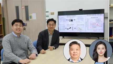
<(From Left) Ph.D. Student Jaejung Park and Professor Seungchul Lee of KAIST Department of Mechanical Engineering and , Professor Hyoung Seop Kim of POSTECH, and M.S.–Ph.D. Integrated Program Student Jeong Ah Lee of POSTECH. >
The KAIST research team led by Professor Seungchul Lee from Department of Mechanical Engineering, in collaboration with Professor Hyoung Seop Kim’s team at POSTECH, successfully overcame the strength–ductility dilemma of Ti 6Al 4V alloy using artificial intelligence, enabling the production of high strength, high ductility metal products. The AI developed by the team accurately predicts mechanical properties based on various 3D printing process parameters while also providing uncertainty information, and it uses both to recommend process parameters that hold high promise for 3D printing.
Among various 3D printing technologies, laser powder bed fusion is an innovative method for manufacturing Ti-6Al-4V alloy, renowned for its high strength and bio-compatibility. However, this alloy made via 3D printing has traditionally faced challenges in simultaneously achieving high strength and high ductility. Although there have been attempts to address this issue by adjusting both the printing process parameters and heat treatment conditions, the vast number of possible combinations made it difficult to explore them all through experiments and simulations alone.
The active learning framework developed by the team quickly explores a wide range of 3D printing process parameters and heat treatment conditions to recommend those expected to improve both strength and ductility of the alloy. These recommendations are based on the AI model’s predictions of ultimate tensile strength and total elongation along with associated uncertainty information for each set of process parameters and heat treatment conditions. The recommended conditions are then validated by performing 3D printing and tensile tests to obtain the true mechanical property values. These new data are incorporated into further AI model training, and through iterative exploration, the optimal process parameters and heat treatment conditions for producing high-performance alloys were determined in only five iterations. With these optimized conditions, the 3D printed Ti-6Al-4V alloy achieved an ultimate tensile strength of 1190 MPa and a total elongation of 16.5%, successfully overcoming the strength–ductility dilemma.
Professor Seungchul Lee commented, “In this study, by optimizing the 3D printing process parameters and heat treatment conditions, we were able to develop a high-strength, high-ductility Ti-6Al-4V alloy with minimal experimentation trials. Compared to previous studies, we produced an alloy with a similar ultimate tensile strength but higher total elongation, as well as that with a similar elongation but greater ultimate tensile strength.” He added, “Furthermore, if our approach is applied not only to mechanical properties but also to other properties such as thermal conductivity and thermal expansion, we anticipate that it will enable efficient exploration of 3D printing process parameters and heat treatment conditions.”
This study was published in Nature Communications on January 22 (https://doi.org/10.1038/s41467-025-56267-1), and the research was supported by the National Research Foundation of Korea’s Nano & Material Technology Development Program and the Leading Research Center Program.
2025.02.21 View 5456
KAIST Research Team Develops an AI Framework Capable of Overcoming the Strength-Ductility Dilemma in Additive-manufactured Titanium Alloys
<(From Left) Ph.D. Student Jaejung Park and Professor Seungchul Lee of KAIST Department of Mechanical Engineering and , Professor Hyoung Seop Kim of POSTECH, and M.S.–Ph.D. Integrated Program Student Jeong Ah Lee of POSTECH. >
The KAIST research team led by Professor Seungchul Lee from Department of Mechanical Engineering, in collaboration with Professor Hyoung Seop Kim’s team at POSTECH, successfully overcame the strength–ductility dilemma of Ti 6Al 4V alloy using artificial intelligence, enabling the production of high strength, high ductility metal products. The AI developed by the team accurately predicts mechanical properties based on various 3D printing process parameters while also providing uncertainty information, and it uses both to recommend process parameters that hold high promise for 3D printing.
Among various 3D printing technologies, laser powder bed fusion is an innovative method for manufacturing Ti-6Al-4V alloy, renowned for its high strength and bio-compatibility. However, this alloy made via 3D printing has traditionally faced challenges in simultaneously achieving high strength and high ductility. Although there have been attempts to address this issue by adjusting both the printing process parameters and heat treatment conditions, the vast number of possible combinations made it difficult to explore them all through experiments and simulations alone.
The active learning framework developed by the team quickly explores a wide range of 3D printing process parameters and heat treatment conditions to recommend those expected to improve both strength and ductility of the alloy. These recommendations are based on the AI model’s predictions of ultimate tensile strength and total elongation along with associated uncertainty information for each set of process parameters and heat treatment conditions. The recommended conditions are then validated by performing 3D printing and tensile tests to obtain the true mechanical property values. These new data are incorporated into further AI model training, and through iterative exploration, the optimal process parameters and heat treatment conditions for producing high-performance alloys were determined in only five iterations. With these optimized conditions, the 3D printed Ti-6Al-4V alloy achieved an ultimate tensile strength of 1190 MPa and a total elongation of 16.5%, successfully overcoming the strength–ductility dilemma.
Professor Seungchul Lee commented, “In this study, by optimizing the 3D printing process parameters and heat treatment conditions, we were able to develop a high-strength, high-ductility Ti-6Al-4V alloy with minimal experimentation trials. Compared to previous studies, we produced an alloy with a similar ultimate tensile strength but higher total elongation, as well as that with a similar elongation but greater ultimate tensile strength.” He added, “Furthermore, if our approach is applied not only to mechanical properties but also to other properties such as thermal conductivity and thermal expansion, we anticipate that it will enable efficient exploration of 3D printing process parameters and heat treatment conditions.”
This study was published in Nature Communications on January 22 (https://doi.org/10.1038/s41467-025-56267-1), and the research was supported by the National Research Foundation of Korea’s Nano & Material Technology Development Program and the Leading Research Center Program.
2025.02.21 View 5456 -
 KAIST Develops Neuromorphic Semiconductor Chip that Learns and Corrects Itself
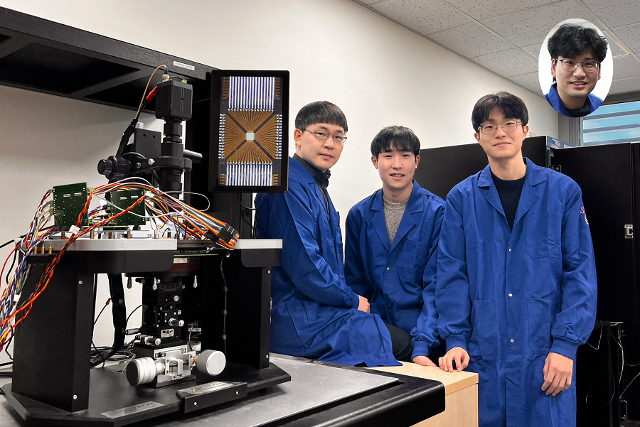
< Photo. The research team of the School of Electrical Engineering posed by the newly deveoped processor. (From center to the right) Professor Young-Gyu Yoon, Integrated Master's and Doctoral Program Students Seungjae Han and Hakcheon Jeong and Professor Shinhyun Choi >
- Professor Shinhyun Choi and Professor Young-Gyu Yoon’s Joint Research Team from the School of Electrical Engineering developed a computing chip that can learn, correct errors, and process AI tasks
- Equipping a computing chip with high-reliability memristor devices with self-error correction functions for real-time learning and image processing
Existing computer systems have separate data processing and storage devices, making them inefficient for processing complex data like AI. A KAIST research team has developed a memristor-based integrated system similar to the way our brain processes information. It is now ready for application in various devices including smart security cameras, allowing them to recognize suspicious activity immediately without having to rely on remote cloud servers, and medical devices with which it can help analyze health data in real time.
KAIST (President Kwang Hyung Lee) announced on the 17th of January that the joint research team of Professor Shinhyun Choi and Professor Young-Gyu Yoon of the School of Electrical Engineering has developed a next-generation neuromorphic semiconductor-based ultra-small computing chip that can learn and correct errors on its own.
< Figure 1. Scanning electron microscope (SEM) image of a computing chip equipped with a highly reliable selector-less 32×32 memristor crossbar array (left). Hardware system developed for real-time artificial intelligence implementation (right). >
What is special about this computing chip is that it can learn and correct errors that occur due to non-ideal characteristics that were difficult to solve in existing neuromorphic devices. For example, when processing a video stream, the chip learns to automatically separate a moving object from the background, and it becomes better at this task over time.
This self-learning ability has been proven by achieving accuracy comparable to ideal computer simulations in real-time image processing. The research team's main achievement is that it has completed a system that is both reliable and practical, beyond the development of brain-like components.
The research team has developed the world's first memristor-based integrated system that can adapt to immediate environmental changes, and has presented an innovative solution that overcomes the limitations of existing technology.
< Figure 2. Background and foreground separation results of an image containing non-ideal characteristics of memristor devices (left). Real-time image separation results through on-device learning using the memristor computing chip developed by our research team (right). >
At the heart of this innovation is a next-generation semiconductor device called a memristor*. The variable resistance characteristics of this device can replace the role of synapses in neural networks, and by utilizing it, data storage and computation can be performed simultaneously, just like our brain cells.
*Memristor: A compound word of memory and resistor, next-generation electrical device whose resistance value is determined by the amount and direction of charge that has flowed between the two terminals in the past.
The research team designed a highly reliable memristor that can precisely control resistance changes and developed an efficient system that excludes complex compensation processes through self-learning. This study is significant in that it experimentally verified the commercialization possibility of a next-generation neuromorphic semiconductor-based integrated system that supports real-time learning and inference.
This technology will revolutionize the way artificial intelligence is used in everyday devices, allowing AI tasks to be processed locally without relying on remote cloud servers, making them faster, more privacy-protected, and more energy-efficient.
“This system is like a smart workspace where everything is within arm’s reach instead of having to go back and forth between desks and file cabinets,” explained KAIST researchers Hakcheon Jeong and Seungjae Han, who led the development of this technology. “This is similar to the way our brain processes information, where everything is processed efficiently at once at one spot.”
The research was conducted with Hakcheon Jeong and Seungjae Han, the students of Integrated Master's and Doctoral Program at KAIST School of Electrical Engineering being the co-first authors, the results of which was published online in the international academic journal, Nature Electronics, on January 8, 2025.
*Paper title: Self-supervised video processing with self-calibration on an analogue computing platform based on a selector-less memristor array ( https://doi.org/10.1038/s41928-024-01318-6 )
This research was supported by the Next-Generation Intelligent Semiconductor Technology Development Project, Excellent New Researcher Project and PIM AI Semiconductor Core Technology Development Project of the National Research Foundation of Korea, and the Electronics and Telecommunications Research Institute Research and Development Support Project of the Institute of Information & communications Technology Planning & Evaluation.
2025.01.17 View 7914
KAIST Develops Neuromorphic Semiconductor Chip that Learns and Corrects Itself
< Photo. The research team of the School of Electrical Engineering posed by the newly deveoped processor. (From center to the right) Professor Young-Gyu Yoon, Integrated Master's and Doctoral Program Students Seungjae Han and Hakcheon Jeong and Professor Shinhyun Choi >
- Professor Shinhyun Choi and Professor Young-Gyu Yoon’s Joint Research Team from the School of Electrical Engineering developed a computing chip that can learn, correct errors, and process AI tasks
- Equipping a computing chip with high-reliability memristor devices with self-error correction functions for real-time learning and image processing
Existing computer systems have separate data processing and storage devices, making them inefficient for processing complex data like AI. A KAIST research team has developed a memristor-based integrated system similar to the way our brain processes information. It is now ready for application in various devices including smart security cameras, allowing them to recognize suspicious activity immediately without having to rely on remote cloud servers, and medical devices with which it can help analyze health data in real time.
KAIST (President Kwang Hyung Lee) announced on the 17th of January that the joint research team of Professor Shinhyun Choi and Professor Young-Gyu Yoon of the School of Electrical Engineering has developed a next-generation neuromorphic semiconductor-based ultra-small computing chip that can learn and correct errors on its own.
< Figure 1. Scanning electron microscope (SEM) image of a computing chip equipped with a highly reliable selector-less 32×32 memristor crossbar array (left). Hardware system developed for real-time artificial intelligence implementation (right). >
What is special about this computing chip is that it can learn and correct errors that occur due to non-ideal characteristics that were difficult to solve in existing neuromorphic devices. For example, when processing a video stream, the chip learns to automatically separate a moving object from the background, and it becomes better at this task over time.
This self-learning ability has been proven by achieving accuracy comparable to ideal computer simulations in real-time image processing. The research team's main achievement is that it has completed a system that is both reliable and practical, beyond the development of brain-like components.
The research team has developed the world's first memristor-based integrated system that can adapt to immediate environmental changes, and has presented an innovative solution that overcomes the limitations of existing technology.
< Figure 2. Background and foreground separation results of an image containing non-ideal characteristics of memristor devices (left). Real-time image separation results through on-device learning using the memristor computing chip developed by our research team (right). >
At the heart of this innovation is a next-generation semiconductor device called a memristor*. The variable resistance characteristics of this device can replace the role of synapses in neural networks, and by utilizing it, data storage and computation can be performed simultaneously, just like our brain cells.
*Memristor: A compound word of memory and resistor, next-generation electrical device whose resistance value is determined by the amount and direction of charge that has flowed between the two terminals in the past.
The research team designed a highly reliable memristor that can precisely control resistance changes and developed an efficient system that excludes complex compensation processes through self-learning. This study is significant in that it experimentally verified the commercialization possibility of a next-generation neuromorphic semiconductor-based integrated system that supports real-time learning and inference.
This technology will revolutionize the way artificial intelligence is used in everyday devices, allowing AI tasks to be processed locally without relying on remote cloud servers, making them faster, more privacy-protected, and more energy-efficient.
“This system is like a smart workspace where everything is within arm’s reach instead of having to go back and forth between desks and file cabinets,” explained KAIST researchers Hakcheon Jeong and Seungjae Han, who led the development of this technology. “This is similar to the way our brain processes information, where everything is processed efficiently at once at one spot.”
The research was conducted with Hakcheon Jeong and Seungjae Han, the students of Integrated Master's and Doctoral Program at KAIST School of Electrical Engineering being the co-first authors, the results of which was published online in the international academic journal, Nature Electronics, on January 8, 2025.
*Paper title: Self-supervised video processing with self-calibration on an analogue computing platform based on a selector-less memristor array ( https://doi.org/10.1038/s41928-024-01318-6 )
This research was supported by the Next-Generation Intelligent Semiconductor Technology Development Project, Excellent New Researcher Project and PIM AI Semiconductor Core Technology Development Project of the National Research Foundation of Korea, and the Electronics and Telecommunications Research Institute Research and Development Support Project of the Institute of Information & communications Technology Planning & Evaluation.
2025.01.17 View 7914 -
 Researchers finds a way to reduce the overheating of semiconductor devices
The demand to shrink the size of semiconductors coupled with the problem of the heat generated at the hot spots of the devices not being effectively dispersed has negatively affected the reliability and durability of modern devices. Existing thermal management technologies have not been up to the task. Thus, the discovery of a new way of dispersing heat by using surface waves generated on the thin metal films over the substrate is an important breakthrough.
KAIST (President Kwang Hyung Lee) announced that Professor Bong Jae Lee's research team in the Department of Mechanical Engineering succeeded in measuring a newly observed transference of heat induced by 'surface plasmon polariton' (SPP) in a thin metal film deposited on a substrate for the first time in the world.
☞ Surface plasmon polariton (SPP) refers to a surface wave formed on the surface of a metal as a result of strong interaction between the electromagnetic field at the interface between the dielectric and the metal and the free electrons on the metal surface and similar collectively vibrating particles.
The research team utilized surface plasmon polaritons (SPP), which are surface waves generated at the metal-dielectric interface, to improve thermal diffusion in nanoscale thin metal films. Since this new heat transfer mode occurs when a thin film of metal is deposited on a substrate, it is highly usable in the device manufacturing process and has the advantage of being able to be manufactured over a large area. The research team showed that the thermal conductivity increased by about 25% due to surface waves generated over a 100-nm-thick titanium (Ti) film with a radius of about 3 cm.
KAIST Professor Bong Jae Lee, who led the research, said, "The significance of this research is that a new heat transfer mode using surface waves over a thin metal film deposited on a substrate with low processing difficulty was identified for the first time in the world. It can be applied as a nanoscale heat spreader to efficiently dissipate heat near the hot spots for easily overheatable semiconductor devices.”
The result has great implications for the development of high-performance semiconductor devices in the future in that it can be applied to rapidly dissipate heat on a nanoscale thin film. In particular, this new heat transfer mode identified by the research team is expected to solve the fundamental problem of thermal management in semiconductor devices as it enables even more effective heat transfer at nanoscale thickness while the thermal conductivity of the thin film usually decreases due to the boundary scattering effect.
This study was published online on April 26 in 'Physical Review Letters' and was selected as an Editors' Suggestion. The research was carried out with support from the Basic Research Laboratory Support Program of the National Research Foundation of Korea.
< Figure. Schematic diagram of the principle of measuring the thermal conductivity of thin Titanium (TI) films and the thermal conductivity of surface plasmon polariton measured on the Ti film >
2023.06.01 View 8934
Researchers finds a way to reduce the overheating of semiconductor devices
The demand to shrink the size of semiconductors coupled with the problem of the heat generated at the hot spots of the devices not being effectively dispersed has negatively affected the reliability and durability of modern devices. Existing thermal management technologies have not been up to the task. Thus, the discovery of a new way of dispersing heat by using surface waves generated on the thin metal films over the substrate is an important breakthrough.
KAIST (President Kwang Hyung Lee) announced that Professor Bong Jae Lee's research team in the Department of Mechanical Engineering succeeded in measuring a newly observed transference of heat induced by 'surface plasmon polariton' (SPP) in a thin metal film deposited on a substrate for the first time in the world.
☞ Surface plasmon polariton (SPP) refers to a surface wave formed on the surface of a metal as a result of strong interaction between the electromagnetic field at the interface between the dielectric and the metal and the free electrons on the metal surface and similar collectively vibrating particles.
The research team utilized surface plasmon polaritons (SPP), which are surface waves generated at the metal-dielectric interface, to improve thermal diffusion in nanoscale thin metal films. Since this new heat transfer mode occurs when a thin film of metal is deposited on a substrate, it is highly usable in the device manufacturing process and has the advantage of being able to be manufactured over a large area. The research team showed that the thermal conductivity increased by about 25% due to surface waves generated over a 100-nm-thick titanium (Ti) film with a radius of about 3 cm.
KAIST Professor Bong Jae Lee, who led the research, said, "The significance of this research is that a new heat transfer mode using surface waves over a thin metal film deposited on a substrate with low processing difficulty was identified for the first time in the world. It can be applied as a nanoscale heat spreader to efficiently dissipate heat near the hot spots for easily overheatable semiconductor devices.”
The result has great implications for the development of high-performance semiconductor devices in the future in that it can be applied to rapidly dissipate heat on a nanoscale thin film. In particular, this new heat transfer mode identified by the research team is expected to solve the fundamental problem of thermal management in semiconductor devices as it enables even more effective heat transfer at nanoscale thickness while the thermal conductivity of the thin film usually decreases due to the boundary scattering effect.
This study was published online on April 26 in 'Physical Review Letters' and was selected as an Editors' Suggestion. The research was carried out with support from the Basic Research Laboratory Support Program of the National Research Foundation of Korea.
< Figure. Schematic diagram of the principle of measuring the thermal conductivity of thin Titanium (TI) films and the thermal conductivity of surface plasmon polariton measured on the Ti film >
2023.06.01 View 8934 -
 Home-Grown Transparent Thin Film Transistor Developed
KAIST, Aug. 6, 2008 -- A KAIST research team led by Profs. Jae-Woo Park and Seung-Hyup Yoo of the Electrical Engineering Division has developed a home-grown technology to create transparent thin film transistor using titanium dioxide., university authorities said.The KAIST team made the technological advance in collaboration with the LCD Division of Samsung Electronics and the Techno Semichem Co., a local LCD equipment maker. Transparent thin film transistor continues to enjoy a wealth of popularity and intensive research interest since it is used in producing operating circuits including transparent display, active-matrix OLED (AMOLED) display and flexible display.
The new technology is significant in that it is based on a titanium dioxide, the first such attempt in the world, while the technologies patented by the United States and Japan are based on ZnO.
Researchers will continue to work on securing technological reliability and developing a technology to mass-produce in a large-scale chemical vapor deposition equipment for the next couple of years.
"The development of technology to produce transparent thin film transistor will help Korean LCD makers reduce its dependence on foreign technologies, as well as maintain Korea"s status as a leader of the world"s display industry," said Prof. Park.
KAIST has applied for local patent registration of the technology and the process is expected to complete by this October or November. International patents have been also applied for in the U.S., Japan and Europe.
The new technology was introduced in the latest edition of the Electron Device Letters, a journal published by the Institute of Electrical and Electronics Engineers or IEEE, a New York-based international non-profit, professional organization for the advancement of technology related to electricity. It will be presented at the International Display Workshop 2008 on Dec. 5 in Niigata, Japan.
2008.08.07 View 18095
Home-Grown Transparent Thin Film Transistor Developed
KAIST, Aug. 6, 2008 -- A KAIST research team led by Profs. Jae-Woo Park and Seung-Hyup Yoo of the Electrical Engineering Division has developed a home-grown technology to create transparent thin film transistor using titanium dioxide., university authorities said.The KAIST team made the technological advance in collaboration with the LCD Division of Samsung Electronics and the Techno Semichem Co., a local LCD equipment maker. Transparent thin film transistor continues to enjoy a wealth of popularity and intensive research interest since it is used in producing operating circuits including transparent display, active-matrix OLED (AMOLED) display and flexible display.
The new technology is significant in that it is based on a titanium dioxide, the first such attempt in the world, while the technologies patented by the United States and Japan are based on ZnO.
Researchers will continue to work on securing technological reliability and developing a technology to mass-produce in a large-scale chemical vapor deposition equipment for the next couple of years.
"The development of technology to produce transparent thin film transistor will help Korean LCD makers reduce its dependence on foreign technologies, as well as maintain Korea"s status as a leader of the world"s display industry," said Prof. Park.
KAIST has applied for local patent registration of the technology and the process is expected to complete by this October or November. International patents have been also applied for in the U.S., Japan and Europe.
The new technology was introduced in the latest edition of the Electron Device Letters, a journal published by the Institute of Electrical and Electronics Engineers or IEEE, a New York-based international non-profit, professional organization for the advancement of technology related to electricity. It will be presented at the International Display Workshop 2008 on Dec. 5 in Niigata, Japan.
2008.08.07 View 18095