Stability
-
 KAIST Develops Wearable Carbon Dioxide Sensor to Enable Real-time Apnea Diagnosis
- Professor Seunghyup Yoo’s research team of the School of Electrical Engineering developed an ultralow-power carbon dioxide (CO2) sensor using a flexible and thin organic photodiode, and succeeded in real-time breathing monitoring by attaching it to a commercial mask
- Wearable devices with features such as low power, high stability, and flexibility can be utilized for early diagnosis of various diseases such as chronic obstructive pulmonary disease and sleep apnea
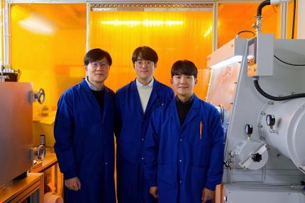
< Photo 1. From the left, School of Electrical Engineering, Ph.D. candidate DongHo Choi, Professor Seunghyup Yoo, and Department of Materials Science and Engineering, Bachelor’s candidate MinJae Kim >
Carbon dioxide (CO2) is a major respiratory metabolite, and continuous monitoring of CO2 concentration in exhaled breath is not only an important indicator for early detection and diagnosis of respiratory and circulatory system diseases, but can also be widely used for monitoring personal exercise status. KAIST researchers succeeded in accurately measuring CO2 concentration by attaching it to the inside of a mask.
KAIST (President Kwang-Hyung Lee) announced on February 10th that Professor Seunghyup Yoo's research team in the Department of Electrical and Electronic Engineering developed a low-power, high-speed wearable CO2 sensor capable of stable breathing monitoring in real time.
Existing non-invasive CO2 sensors had limitations in that they were large in size and consumed high power. In particular, optochemical CO2 sensors using fluorescent molecules have the advantage of being miniaturized and lightweight, but due to the photodegradation phenomenon of dye molecules, they are difficult to use stably for a long time, which limits their use as wearable healthcare sensors.
Optochemical CO2 sensors utilize the fact that the intensity of fluorescence emitted from fluorescent molecules decreases depending on the concentration of CO2, and it is important to effectively detect changes in fluorescence light.
To this end, the research team developed a low-power CO2 sensor consisting of an LED and an organic photodiode surrounding it. Based on high light collection efficiency, the sensor, which minimizes the amount of excitation light irradiated on fluorescent molecules, achieved a device power consumption of 171 μW, which is tens of times lower than existing sensors that consume several mW.
< Figure 1. Structure and operating principle of the developed optochemical carbon dioxide (CO2) sensor. Light emitted from the LED is converted into fluorescence through the fluorescent film, reflected from the light scattering layer, and incident on the organic photodiode. CO2 reacts with a small amount of water inside the fluorescent film to form carbonic acid (H2CO3), which increases the concentration of hydrogen ions (H+), and the fluorescence intensity due to 470 nm excitation light decreases. The circular organic photodiode with high light collection efficiency effectively detects changes in fluorescence intensity, lowers the power required light up the LED, and reduces light-induced deterioration. >
The research team also elucidated the photodegradation path of fluorescent molecules used in CO2 sensors, revealed the cause of the increase in error over time in photochemical sensors, and suggested an optical design method to suppress the occurrence of errors.
Based on this, the research team developed a sensor that effectively reduces errors caused by photodegradation, which was a chronic problem of existing photochemical sensors, and can be used continuously for up to 9 hours while existing technologies based on the same material can be used for less than 20 minutes, and can be used multiple times when replacing the CO2 detection fluorescent film.
< Figure 2. Wearable smart mask and real-time breathing monitoring. The fabricated sensor module consists of four elements (①: gas-permeable light-scattering layer, ②: color filter and organic photodiode, ③: light-emitting diode, ④: CO2-detecting fluorescent film). The thin and light sensor (D1: 400 nm, D2: 470 nm) is attached to the inside of the mask to monitor the wearer's breathing in real time. >
The developed sensor accurately measured CO2 concentration by being attached to the inside of a mask based on the advantages of being light (0.12 g), thin (0.7 mm), and flexible. In addition, it showed fast speed and high resolution that can monitor respiratory rate by distinguishing between inhalation and exhalation in real time.
< Photo 2. The developed sensor attached to the inside of the mask >
Professor Seunghyup Yoo said, "The developed sensor has excellent characteristics such as low power, high stability, and flexibility, so it can be widely applied to wearable devices, and can be used for the early diagnosis of various diseases such as hypercapnia, chronic obstructive pulmonary disease, and sleep apnea." He added, "In particular, it is expected to be used to improve side effects caused by rebreathing in environments where dust is generated or where masks are worn for long periods of time, such as during seasonal changes."
This study, in which KAIST's Department of Materials Science and Engineering's undergraduate student Minjae Kim and School of Electrical Engineering's doctoral student Dongho Choi participated as joint first authors, was published in the online version of Cell's sister journal, Device, on the 22nd of last month. (Paper title: Ultralow-power carbon dioxide sensor for real-time breath monitoring) DOI: https://doi.org/10.1016/j.device.2024.100681
< Photo 3. From the left, Professor Seunghyup Yoo of the School of Electrical Engineering, MinJae Kim, an undergraduate student in the Department of Materials Science and Engineering, and Dongho Choi, a doctoral student in the School of Electrical Engineering >
This study was supported by the Ministry of Trade, Industry and Energy's Materials and Components Technology Development Project, the National Research Foundation of Korea's Original Technology Development Project, and the KAIST Undergraduate Research Participation Project. This work was supported by the (URP) program.
2025.02.13 View 9078
KAIST Develops Wearable Carbon Dioxide Sensor to Enable Real-time Apnea Diagnosis
- Professor Seunghyup Yoo’s research team of the School of Electrical Engineering developed an ultralow-power carbon dioxide (CO2) sensor using a flexible and thin organic photodiode, and succeeded in real-time breathing monitoring by attaching it to a commercial mask
- Wearable devices with features such as low power, high stability, and flexibility can be utilized for early diagnosis of various diseases such as chronic obstructive pulmonary disease and sleep apnea
< Photo 1. From the left, School of Electrical Engineering, Ph.D. candidate DongHo Choi, Professor Seunghyup Yoo, and Department of Materials Science and Engineering, Bachelor’s candidate MinJae Kim >
Carbon dioxide (CO2) is a major respiratory metabolite, and continuous monitoring of CO2 concentration in exhaled breath is not only an important indicator for early detection and diagnosis of respiratory and circulatory system diseases, but can also be widely used for monitoring personal exercise status. KAIST researchers succeeded in accurately measuring CO2 concentration by attaching it to the inside of a mask.
KAIST (President Kwang-Hyung Lee) announced on February 10th that Professor Seunghyup Yoo's research team in the Department of Electrical and Electronic Engineering developed a low-power, high-speed wearable CO2 sensor capable of stable breathing monitoring in real time.
Existing non-invasive CO2 sensors had limitations in that they were large in size and consumed high power. In particular, optochemical CO2 sensors using fluorescent molecules have the advantage of being miniaturized and lightweight, but due to the photodegradation phenomenon of dye molecules, they are difficult to use stably for a long time, which limits their use as wearable healthcare sensors.
Optochemical CO2 sensors utilize the fact that the intensity of fluorescence emitted from fluorescent molecules decreases depending on the concentration of CO2, and it is important to effectively detect changes in fluorescence light.
To this end, the research team developed a low-power CO2 sensor consisting of an LED and an organic photodiode surrounding it. Based on high light collection efficiency, the sensor, which minimizes the amount of excitation light irradiated on fluorescent molecules, achieved a device power consumption of 171 μW, which is tens of times lower than existing sensors that consume several mW.
< Figure 1. Structure and operating principle of the developed optochemical carbon dioxide (CO2) sensor. Light emitted from the LED is converted into fluorescence through the fluorescent film, reflected from the light scattering layer, and incident on the organic photodiode. CO2 reacts with a small amount of water inside the fluorescent film to form carbonic acid (H2CO3), which increases the concentration of hydrogen ions (H+), and the fluorescence intensity due to 470 nm excitation light decreases. The circular organic photodiode with high light collection efficiency effectively detects changes in fluorescence intensity, lowers the power required light up the LED, and reduces light-induced deterioration. >
The research team also elucidated the photodegradation path of fluorescent molecules used in CO2 sensors, revealed the cause of the increase in error over time in photochemical sensors, and suggested an optical design method to suppress the occurrence of errors.
Based on this, the research team developed a sensor that effectively reduces errors caused by photodegradation, which was a chronic problem of existing photochemical sensors, and can be used continuously for up to 9 hours while existing technologies based on the same material can be used for less than 20 minutes, and can be used multiple times when replacing the CO2 detection fluorescent film.
< Figure 2. Wearable smart mask and real-time breathing monitoring. The fabricated sensor module consists of four elements (①: gas-permeable light-scattering layer, ②: color filter and organic photodiode, ③: light-emitting diode, ④: CO2-detecting fluorescent film). The thin and light sensor (D1: 400 nm, D2: 470 nm) is attached to the inside of the mask to monitor the wearer's breathing in real time. >
The developed sensor accurately measured CO2 concentration by being attached to the inside of a mask based on the advantages of being light (0.12 g), thin (0.7 mm), and flexible. In addition, it showed fast speed and high resolution that can monitor respiratory rate by distinguishing between inhalation and exhalation in real time.
< Photo 2. The developed sensor attached to the inside of the mask >
Professor Seunghyup Yoo said, "The developed sensor has excellent characteristics such as low power, high stability, and flexibility, so it can be widely applied to wearable devices, and can be used for the early diagnosis of various diseases such as hypercapnia, chronic obstructive pulmonary disease, and sleep apnea." He added, "In particular, it is expected to be used to improve side effects caused by rebreathing in environments where dust is generated or where masks are worn for long periods of time, such as during seasonal changes."
This study, in which KAIST's Department of Materials Science and Engineering's undergraduate student Minjae Kim and School of Electrical Engineering's doctoral student Dongho Choi participated as joint first authors, was published in the online version of Cell's sister journal, Device, on the 22nd of last month. (Paper title: Ultralow-power carbon dioxide sensor for real-time breath monitoring) DOI: https://doi.org/10.1016/j.device.2024.100681
< Photo 3. From the left, Professor Seunghyup Yoo of the School of Electrical Engineering, MinJae Kim, an undergraduate student in the Department of Materials Science and Engineering, and Dongho Choi, a doctoral student in the School of Electrical Engineering >
This study was supported by the Ministry of Trade, Industry and Energy's Materials and Components Technology Development Project, the National Research Foundation of Korea's Original Technology Development Project, and the KAIST Undergraduate Research Participation Project. This work was supported by the (URP) program.
2025.02.13 View 9078 -
 A System for Stable Simultaneous Communication among Thousands of IoT Devices
A mmWave Backscatter System, developed by a team led by Professor Song Min Kim is exciting news for the IoT market as it will be able to provide fast and stable connectivity even for a massive network, which could finally allow IoT devices to reach their full potential.
A research team led by Professor Song Min Kim of the KAIST School of Electrical Engineering developed a system that can support concurrent communications for tens of millions of IoT devices using backscattering millimeter-level waves (mmWave).
With their mmWave backscatter method, the research team built a design enabling simultaneous signal demodulation in a complex environment for communication where tens of thousands of IoT devices are arranged indoors. The wide frequency range of mmWave exceeds 10GHz, which provides great scalability. In addition, backscattering reflects radiated signals instead of wirelessly creating its own, which allows operation at ultralow power. Therefore, the mmWave backscatter system offers internet connectivity on a mass scale to IoT devices at a low installation cost.
This research by Kangmin Bae et al. was presented at ACM MobiSys 2022. At this world-renowned conference for mobile systems, the research won the Best Paper Award under the title “OmniScatter: Sensitivity mmWave Backscattering Using Commodity FMCW Radar”. It is meaningful that members of the KAIST School of Electrical Engineering have won the Best Paper Award at ACM MobiSys for two consecutive years, as last year was the first time the award was presented to an institute from Asia.
IoT, as a core component of 5G/6G network, is showing exponential growth, and is expected to be part of a trillion devices by 2035. To support the connection of IoT devices on a mass scale, 5G and 6G each aim to support ten times and 100 times the network density of 4G, respectively. As a result, the importance of practical systems for large-scale communication has been raised.
The mmWave is a next-generation communication technology that can be incorporated in 5G/6G standards, as it utilizes carrier waves at frequencies between 30 to 300GHz. However, due to signal reduction at high frequencies and reflection loss, the current mmWave backscatter system enables communication in limited environments. In other words, it cannot operate in complex environments where various obstacles and reflectors are present. As a result, it is limited to the large-scale connection of IoT devices that require a relatively free arrangement.
The research team found the solution in the high coding gain of an FMCW radar. The team developed a signal processing method that can fundamentally separate backscatter signals from ambient noise while maintaining the coding gain of the radar. They achieved a receiver sensitivity of over 100 thousand times that of previously reported FMCW radars, which can support communication in practical environments. Additionally, given the radar’s property where the frequency of the demodulated signal changes depending on the physical location of the tag, the team designed a system that passively assigns them channels. This lets the ultralow-power backscatter communication system to take full advantage of the frequency range at 10 GHz or higher.
The developed system can use the radar of existing commercial products as gateway, making it easily compatible. In addition, since the backscatter system works at ultralow power levels of 10uW or below, it can operate for over 40 years with a single button cell and drastically reduce installation and maintenance costs.
The research team confirmed that mmWave backscatter devices arranged randomly in an office with various obstacles and reflectors could communicate effectively. The team then took things one step further and conducted a successful trace-driven evaluation where they simultaneously received information sent by 1,100 devices.
Their research presents connectivity that greatly exceeds network density required by next-generation communication like 5G and 6G. The system is expected to become a stepping stone for the hyper-connected future to come.
Professor Kim said, “mmWave backscatter is the technology we’ve dreamt of. The mass scalability and ultralow power at which it can operate IoT devices is unmatched by any existing technology”. He added, “We look forward to this system being actively utilized to enable the wide availability of IoT in the hyper-connected generation to come”.
To demonstrate the massive connectivity of the system, a trace-driven evaluation of 1,100 concurrent tag transmissions are made. Figure shows the demodulation result of each and every 1,100 tags as red triangles, where they successfully communicate without collision.
This work was supported by Samsung Research Funding & Incubation Center of Samsung Electronics and by the ITRC (Information Technology Research Center) support program supervised by the IITP (Institute of Information & Communications Technology Planning & Evaluation).
Profile: Song Min Kim, Ph.D.Professorsongmin@kaist.ac.krhttps://smile.kaist.ac.kr
SMILE Lab.School of Electrical Engineering
2022.07.28 View 12537
A System for Stable Simultaneous Communication among Thousands of IoT Devices
A mmWave Backscatter System, developed by a team led by Professor Song Min Kim is exciting news for the IoT market as it will be able to provide fast and stable connectivity even for a massive network, which could finally allow IoT devices to reach their full potential.
A research team led by Professor Song Min Kim of the KAIST School of Electrical Engineering developed a system that can support concurrent communications for tens of millions of IoT devices using backscattering millimeter-level waves (mmWave).
With their mmWave backscatter method, the research team built a design enabling simultaneous signal demodulation in a complex environment for communication where tens of thousands of IoT devices are arranged indoors. The wide frequency range of mmWave exceeds 10GHz, which provides great scalability. In addition, backscattering reflects radiated signals instead of wirelessly creating its own, which allows operation at ultralow power. Therefore, the mmWave backscatter system offers internet connectivity on a mass scale to IoT devices at a low installation cost.
This research by Kangmin Bae et al. was presented at ACM MobiSys 2022. At this world-renowned conference for mobile systems, the research won the Best Paper Award under the title “OmniScatter: Sensitivity mmWave Backscattering Using Commodity FMCW Radar”. It is meaningful that members of the KAIST School of Electrical Engineering have won the Best Paper Award at ACM MobiSys for two consecutive years, as last year was the first time the award was presented to an institute from Asia.
IoT, as a core component of 5G/6G network, is showing exponential growth, and is expected to be part of a trillion devices by 2035. To support the connection of IoT devices on a mass scale, 5G and 6G each aim to support ten times and 100 times the network density of 4G, respectively. As a result, the importance of practical systems for large-scale communication has been raised.
The mmWave is a next-generation communication technology that can be incorporated in 5G/6G standards, as it utilizes carrier waves at frequencies between 30 to 300GHz. However, due to signal reduction at high frequencies and reflection loss, the current mmWave backscatter system enables communication in limited environments. In other words, it cannot operate in complex environments where various obstacles and reflectors are present. As a result, it is limited to the large-scale connection of IoT devices that require a relatively free arrangement.
The research team found the solution in the high coding gain of an FMCW radar. The team developed a signal processing method that can fundamentally separate backscatter signals from ambient noise while maintaining the coding gain of the radar. They achieved a receiver sensitivity of over 100 thousand times that of previously reported FMCW radars, which can support communication in practical environments. Additionally, given the radar’s property where the frequency of the demodulated signal changes depending on the physical location of the tag, the team designed a system that passively assigns them channels. This lets the ultralow-power backscatter communication system to take full advantage of the frequency range at 10 GHz or higher.
The developed system can use the radar of existing commercial products as gateway, making it easily compatible. In addition, since the backscatter system works at ultralow power levels of 10uW or below, it can operate for over 40 years with a single button cell and drastically reduce installation and maintenance costs.
The research team confirmed that mmWave backscatter devices arranged randomly in an office with various obstacles and reflectors could communicate effectively. The team then took things one step further and conducted a successful trace-driven evaluation where they simultaneously received information sent by 1,100 devices.
Their research presents connectivity that greatly exceeds network density required by next-generation communication like 5G and 6G. The system is expected to become a stepping stone for the hyper-connected future to come.
Professor Kim said, “mmWave backscatter is the technology we’ve dreamt of. The mass scalability and ultralow power at which it can operate IoT devices is unmatched by any existing technology”. He added, “We look forward to this system being actively utilized to enable the wide availability of IoT in the hyper-connected generation to come”.
To demonstrate the massive connectivity of the system, a trace-driven evaluation of 1,100 concurrent tag transmissions are made. Figure shows the demodulation result of each and every 1,100 tags as red triangles, where they successfully communicate without collision.
This work was supported by Samsung Research Funding & Incubation Center of Samsung Electronics and by the ITRC (Information Technology Research Center) support program supervised by the IITP (Institute of Information & Communications Technology Planning & Evaluation).
Profile: Song Min Kim, Ph.D.Professorsongmin@kaist.ac.krhttps://smile.kaist.ac.kr
SMILE Lab.School of Electrical Engineering
2022.07.28 View 12537 -
 Success in Real-Time Observation of the Formation Process of Topological Solitons, a Core Technology for Next-Generation Information Transfer
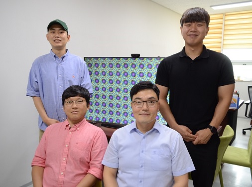
< From left) Geonhyeong Park (Ph.D. Candidate), Yun-Seok Choi (Ph.D.), Professor Dong Ki Yoon, and Changjae Lee (Ph.D. Candidate) of the Department of Chemistry >
Professor Dong Ki Yoon's research team in the Department of Chemistry at KAIST announced on the 11th that they have succeeded in controlling the formation of topological solitons in a regular, large-area manner through the self-assembly of chiral liquid crystal materials and observing their formation process in real-time.
A soliton refers to a phenomenon where a specific wave persists without dissipating through interaction with its surroundings. In particular, even when a wave is transmitted over long distances, it retains its unique information until it reaches the desired destination. Therefore, in today's digital society, which is susceptible to hacking, solitons are highly anticipated to be the core of future communication due to their inherent high stability. Furthermore, topological solitons created using organic liquid crystal molecules are expected to be utilized as next-generation anti-counterfeiting devices and memory elements due to their unique spin directionality.
Professor Yoon's team specifically revealed the formation process of topological solitons in this study, which had not been observable in real-time under mild conditions such as room temperature until now. This was made possible by using self-assembling chiral liquid crystal materials in a confined space created by air pillars.
This research, in which Geonhyeong Park (Ph.D. Candidate, Department of Chemistry) and Dr. Ahram Suh participated as co-first authors, and Dr. Yun-Seok Choi and Changjae Lee (Ph.D. Candidate) from the same group also participated, was published online in the international journal 'Advanced Materials' on June 5th and is scheduled to be featured as the back cover of the July issue. (Paper title: "Fabrication of Arrays of Topological Solitons in Patterned Chiral Liquid Crystals for Real-Time Observation of Morphogenesis")
< Figure 1. Schematic diagram of the research>
< Figure 2. Real-time observation of topological soliton formation using liquid crystals>
In this study, Professor Yoon's team implemented topological soliton structures at approximately 30 degrees Celsius, similar to room temperature, using chiral (asymmetric) liquid crystal materials instead of the conventional liquid crystal molecules widely used as core materials in liquid crystal displays (LCDs). Generally, complex equipment is required to control the formation of topological solitons, and their formation time is very short, which has hindered research into their formation process until now.
To achieve regular formation and control of topological solitons formed by chiral liquid crystal molecules, Professor Yoon's team precisely controlled a combination of vertical alignment layers, which can orient molecules vertically, and air pillars. Specifically, they prepared concave patterns based on circular silicon material, several micrometers (one-millionth of a meter) in size, coated with a vertical alignment layer, and a glass substrate. By adjusting the gap to several micrometers and injecting chiral liquid crystal material, air pillars were spontaneously formed on the concave patterns. Subsequently, the liquid crystal molecules were vertically aligned on all substrates, inevitably causing regular distortions between the substrates, and between the substrate and the air pillars, thus developing a system where chiral molecular structures, i.e., topological solitons, could be formed.
The key to the formation and control of topological solitons lies in controlling the thermal phase transition to occur regularly as desired when cooling from the isotropic phase temperature (approximately 40 degrees Celsius) to the liquid crystal phase temperature (approximately 30 degrees Celsius), where the liquid crystal material near the air pillars is cooler than the liquid crystal material between the glass substrate and the silicon patterned parts. This is consistent with the everyday wisdom of eating steamed eggs from a 'Ttukbaegi' (earthen pot) by starting from the relatively cooler part exposed to the air (near the air pillars) rather than the hot pot part (silicon or glass substrate part).
Through real-time analysis, the research team elucidated that topological defects are formed by the naturally formed air pillars through controlled thermal phase transition, and topological solitons are formed only at the locations of these defects. This analysis technique has the potential for application in various fields, including the interpretation of topological soliton formation found in other physical phenomena such as skyrmion particles in electromagnetism.
< Figure 3. Snapshots during the formation process of regularly arranged topological solitons>
Professor Dong Ki Yoon stated, "General topological solitons are known to be highly stable, capable only of generation or annihilation. Through the results of this research, we can understand the formation process of solitons in more detail, and they can be used as spintronics application technology, considered a next-generation semiconductor device for storing and recording information."
This research was conducted in collaboration with Professor Ivan Smalyukh's laboratory at the University of Colorado, Department of Physics, and was supported by the Multiscale Chiral Structures Research Center and strategic projects of the National Research Foundation of Korea under the Ministry of Science and ICT.
2022.07.11 View 1541
Success in Real-Time Observation of the Formation Process of Topological Solitons, a Core Technology for Next-Generation Information Transfer
< From left) Geonhyeong Park (Ph.D. Candidate), Yun-Seok Choi (Ph.D.), Professor Dong Ki Yoon, and Changjae Lee (Ph.D. Candidate) of the Department of Chemistry >
Professor Dong Ki Yoon's research team in the Department of Chemistry at KAIST announced on the 11th that they have succeeded in controlling the formation of topological solitons in a regular, large-area manner through the self-assembly of chiral liquid crystal materials and observing their formation process in real-time.
A soliton refers to a phenomenon where a specific wave persists without dissipating through interaction with its surroundings. In particular, even when a wave is transmitted over long distances, it retains its unique information until it reaches the desired destination. Therefore, in today's digital society, which is susceptible to hacking, solitons are highly anticipated to be the core of future communication due to their inherent high stability. Furthermore, topological solitons created using organic liquid crystal molecules are expected to be utilized as next-generation anti-counterfeiting devices and memory elements due to their unique spin directionality.
Professor Yoon's team specifically revealed the formation process of topological solitons in this study, which had not been observable in real-time under mild conditions such as room temperature until now. This was made possible by using self-assembling chiral liquid crystal materials in a confined space created by air pillars.
This research, in which Geonhyeong Park (Ph.D. Candidate, Department of Chemistry) and Dr. Ahram Suh participated as co-first authors, and Dr. Yun-Seok Choi and Changjae Lee (Ph.D. Candidate) from the same group also participated, was published online in the international journal 'Advanced Materials' on June 5th and is scheduled to be featured as the back cover of the July issue. (Paper title: "Fabrication of Arrays of Topological Solitons in Patterned Chiral Liquid Crystals for Real-Time Observation of Morphogenesis")
< Figure 1. Schematic diagram of the research>
< Figure 2. Real-time observation of topological soliton formation using liquid crystals>
In this study, Professor Yoon's team implemented topological soliton structures at approximately 30 degrees Celsius, similar to room temperature, using chiral (asymmetric) liquid crystal materials instead of the conventional liquid crystal molecules widely used as core materials in liquid crystal displays (LCDs). Generally, complex equipment is required to control the formation of topological solitons, and their formation time is very short, which has hindered research into their formation process until now.
To achieve regular formation and control of topological solitons formed by chiral liquid crystal molecules, Professor Yoon's team precisely controlled a combination of vertical alignment layers, which can orient molecules vertically, and air pillars. Specifically, they prepared concave patterns based on circular silicon material, several micrometers (one-millionth of a meter) in size, coated with a vertical alignment layer, and a glass substrate. By adjusting the gap to several micrometers and injecting chiral liquid crystal material, air pillars were spontaneously formed on the concave patterns. Subsequently, the liquid crystal molecules were vertically aligned on all substrates, inevitably causing regular distortions between the substrates, and between the substrate and the air pillars, thus developing a system where chiral molecular structures, i.e., topological solitons, could be formed.
The key to the formation and control of topological solitons lies in controlling the thermal phase transition to occur regularly as desired when cooling from the isotropic phase temperature (approximately 40 degrees Celsius) to the liquid crystal phase temperature (approximately 30 degrees Celsius), where the liquid crystal material near the air pillars is cooler than the liquid crystal material between the glass substrate and the silicon patterned parts. This is consistent with the everyday wisdom of eating steamed eggs from a 'Ttukbaegi' (earthen pot) by starting from the relatively cooler part exposed to the air (near the air pillars) rather than the hot pot part (silicon or glass substrate part).
Through real-time analysis, the research team elucidated that topological defects are formed by the naturally formed air pillars through controlled thermal phase transition, and topological solitons are formed only at the locations of these defects. This analysis technique has the potential for application in various fields, including the interpretation of topological soliton formation found in other physical phenomena such as skyrmion particles in electromagnetism.
< Figure 3. Snapshots during the formation process of regularly arranged topological solitons>
Professor Dong Ki Yoon stated, "General topological solitons are known to be highly stable, capable only of generation or annihilation. Through the results of this research, we can understand the formation process of solitons in more detail, and they can be used as spintronics application technology, considered a next-generation semiconductor device for storing and recording information."
This research was conducted in collaboration with Professor Ivan Smalyukh's laboratory at the University of Colorado, Department of Physics, and was supported by the Multiscale Chiral Structures Research Center and strategic projects of the National Research Foundation of Korea under the Ministry of Science and ICT.
2022.07.11 View 1541