SCIE
-
 Material Innovation Realized with Robotic Arms and AI, Without Human Researchers
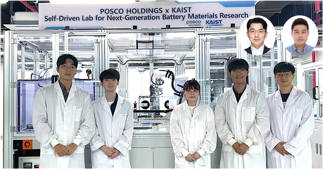
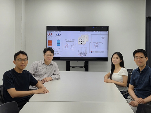
<(From Left) M.S candidate Dongwoo Kim from KAIST, Ph.D candidate Hyun-Gi Lee from KAIST, Intern Yeham Kang from KAIST, M.S candidate Seongjae Bae from KAIST, Professor Dong-Hwa Seo from KAIST, (From top right, from left) Senior Researcher Inchul Park from POSCO Holdings, Senior Researcher Jung Woo Park, senior researcher from POSCO Holdings>
A joint research team from industry and academia in Korea has successfully developed an autonomous lab that uses AI and automation to create new cathode materials for secondary batteries. This system operates without human intervention, drastically reducing researcher labor and cutting the material discovery period by 93%.
* Autonomous Lab: A platform that autonomously designs, conducts, and analyzes experiments to find the optimal material.
KAIST (President Kwang Hyung Lee) announced on the 3rd of August that the research team led by Professor Dong-Hwa Seo of the Department of Materials Science and Engineering, in collaboration with the team of LIB Materials Research Center in Energy Materials R&D Laboratories at POSCO Holdings' POSCO N.EX.T Hub (Director Ki Soo Kim), built the lab to explore cathode materials using AI and automation technology.
Developing secondary battery cathode materials is a labor-intensive and time-consuming process for skilled researchers. It involves extensive exploration of various compositions and experimental variables through weighing, transporting, mixing, sintering*, and analyzing samples.
* Sintering: A process in which powder particles are heated to form a single solid mass through thermal activation.
The research team's autonomous lab combines an automated system with an AI model. The system handles all experimental steps—weighing, mixing, pelletizing, sintering, and analysis—without human interference. The AI model then interprets the data, learns from it, and selects the best candidates for the next experiment.
<Figure 1. Outline of the Anode Material Autonomous Exploration Laboratory>
To increase efficiency, the team designed the automation system with separate modules for each process, which are managed by a central robotic arm. This modular approach reduces the system's reliance on the robotic arm.
The team also significantly improved the synthesis speed by using a new high-speed sintering method, which is 50 times faster than the conventional low-speed method. This allows the autonomous lab to acquire 12 times more material data compared to traditional, researcher-led experiments.
<Figure 2. Synthesis of Cathode Material Using a High-Speed Sintering Device>
The vast amount of data collected is automatically interpreted by the AI model to extract information such as synthesized phases and impurity ratios. This data is systematically stored to create a high-quality database, which then serves as training data for an optimization AI model. This creates a closed-loop experimental system that recommends the next cathode composition and synthesis conditions for the automated system.
* Closed-loop experimental system: A system that independently performs all experimental processes without researcher intervention.
Operating this intelligent automation system 24 hours a day can secure more than 12 times the experimental data and shorten material discovery time by 93%. For a project requiring 500 experiments, the system can complete the work in about 6 days, whereas a traditional researcher-led approach would take 84 days.
During development, POSCO Holdings team managed the overall project planning, reviewed the platform design, and co-developed the partial module design and AI-based experimental model. The KAIST team, led by Professor Dong-hwa Seo, was responsible for the actual system implementation and operation, including platform design, module fabrication, algorithm creation, and system verification and improvement.
Professor Dong-Hwa Seo of KAIST stated that this system is a solution to the decrease in research personnel due to the low birth rate in Korea. He expects it will enhance global competitiveness by accelerating secondary battery material development through the acquisition of high-quality data.
<Figure 3. Exterior View (Side) of the Cathode Material Autonomous Exploration Laboratory>
POSCO N.EX.T Hub plans to apply an upgraded version of this autonomous lab to its own research facilities after 2026 to dramatically speed up next-generation secondary battery material development. They are planning further developments to enhance the system's stability and scalability, and hope this industry-academia collaboration will serve as a model for using innovative technology in real-world R&D.
<Figure 4. Exterior View (Front) of the Cathode Material Autonomous Exploration Laboratory>
The research was spearheaded by Ph.D. student Hyun-Gi Lee, along with master's students Seongjae Bae and Dongwoo Kim from Professor Dong-Hwa Seo’s lab at KAIST. Senior researchers Jung Woo Park and Inchul Park from LIB Materials Research Center of POSCO N.EX.T Hub's Energy Materials R&D Laboratories (Director Jeongjin Hong) also participated.
2025.08.06 View 279
Material Innovation Realized with Robotic Arms and AI, Without Human Researchers
<(From Left) M.S candidate Dongwoo Kim from KAIST, Ph.D candidate Hyun-Gi Lee from KAIST, Intern Yeham Kang from KAIST, M.S candidate Seongjae Bae from KAIST, Professor Dong-Hwa Seo from KAIST, (From top right, from left) Senior Researcher Inchul Park from POSCO Holdings, Senior Researcher Jung Woo Park, senior researcher from POSCO Holdings>
A joint research team from industry and academia in Korea has successfully developed an autonomous lab that uses AI and automation to create new cathode materials for secondary batteries. This system operates without human intervention, drastically reducing researcher labor and cutting the material discovery period by 93%.
* Autonomous Lab: A platform that autonomously designs, conducts, and analyzes experiments to find the optimal material.
KAIST (President Kwang Hyung Lee) announced on the 3rd of August that the research team led by Professor Dong-Hwa Seo of the Department of Materials Science and Engineering, in collaboration with the team of LIB Materials Research Center in Energy Materials R&D Laboratories at POSCO Holdings' POSCO N.EX.T Hub (Director Ki Soo Kim), built the lab to explore cathode materials using AI and automation technology.
Developing secondary battery cathode materials is a labor-intensive and time-consuming process for skilled researchers. It involves extensive exploration of various compositions and experimental variables through weighing, transporting, mixing, sintering*, and analyzing samples.
* Sintering: A process in which powder particles are heated to form a single solid mass through thermal activation.
The research team's autonomous lab combines an automated system with an AI model. The system handles all experimental steps—weighing, mixing, pelletizing, sintering, and analysis—without human interference. The AI model then interprets the data, learns from it, and selects the best candidates for the next experiment.
<Figure 1. Outline of the Anode Material Autonomous Exploration Laboratory>
To increase efficiency, the team designed the automation system with separate modules for each process, which are managed by a central robotic arm. This modular approach reduces the system's reliance on the robotic arm.
The team also significantly improved the synthesis speed by using a new high-speed sintering method, which is 50 times faster than the conventional low-speed method. This allows the autonomous lab to acquire 12 times more material data compared to traditional, researcher-led experiments.
<Figure 2. Synthesis of Cathode Material Using a High-Speed Sintering Device>
The vast amount of data collected is automatically interpreted by the AI model to extract information such as synthesized phases and impurity ratios. This data is systematically stored to create a high-quality database, which then serves as training data for an optimization AI model. This creates a closed-loop experimental system that recommends the next cathode composition and synthesis conditions for the automated system.
* Closed-loop experimental system: A system that independently performs all experimental processes without researcher intervention.
Operating this intelligent automation system 24 hours a day can secure more than 12 times the experimental data and shorten material discovery time by 93%. For a project requiring 500 experiments, the system can complete the work in about 6 days, whereas a traditional researcher-led approach would take 84 days.
During development, POSCO Holdings team managed the overall project planning, reviewed the platform design, and co-developed the partial module design and AI-based experimental model. The KAIST team, led by Professor Dong-hwa Seo, was responsible for the actual system implementation and operation, including platform design, module fabrication, algorithm creation, and system verification and improvement.
Professor Dong-Hwa Seo of KAIST stated that this system is a solution to the decrease in research personnel due to the low birth rate in Korea. He expects it will enhance global competitiveness by accelerating secondary battery material development through the acquisition of high-quality data.
<Figure 3. Exterior View (Side) of the Cathode Material Autonomous Exploration Laboratory>
POSCO N.EX.T Hub plans to apply an upgraded version of this autonomous lab to its own research facilities after 2026 to dramatically speed up next-generation secondary battery material development. They are planning further developments to enhance the system's stability and scalability, and hope this industry-academia collaboration will serve as a model for using innovative technology in real-world R&D.
<Figure 4. Exterior View (Front) of the Cathode Material Autonomous Exploration Laboratory>
The research was spearheaded by Ph.D. student Hyun-Gi Lee, along with master's students Seongjae Bae and Dongwoo Kim from Professor Dong-Hwa Seo’s lab at KAIST. Senior researchers Jung Woo Park and Inchul Park from LIB Materials Research Center of POSCO N.EX.T Hub's Energy Materials R&D Laboratories (Director Jeongjin Hong) also participated.
2025.08.06 View 279 -
 Immune Signals Directly Modulate Brain's Emotional Circuits: Unraveling the Mechanism Behind Anxiety-Inducing Behaviors
KAIST's Department of Brain and Cognitive Sciences, led by Professor Jeong-Tae Kwon, has collaborated with MIT and Harvard Medical School to make a groundbreaking discovery. For the first time globally, their joint research has revealed that cytokines, released during immune responses, directly influence the brain's emotional circuits to regulate anxiety behavior.
The study provided experimental evidence for a bidirectional regulatory mechanism: inflammatory cytokines IL-17A and IL-17C act on specific neurons in the amygdala, a region known for emotional regulation, increasing their excitability and consequently inducing anxiety. Conversely, the anti-inflammatory cytokine IL-10 was found to suppress excitability in these very same neurons, thereby contributing to anxiety alleviation.
In a mouse model, the research team observed that while skin inflammation was mitigated by immunotherapy (IL-17RA antibody), anxiety levels paradoxically rose. This was attributed to elevated circulating IL-17 family cytokines leading to the overactivation of amygdala neurons.
Key finding: Inflammatory cytokines IL-17A/17C promote anxiety by acting on excitable amygdala neurons (via IL-17RA/RE receptors), whereas anti-inflammatory cytokine IL-10 alleviates anxiety by suppressing excitability through IL-10RA receptors on the same neurons.
The researchers further elucidated that the anti-inflammatory cytokine IL-10 works to reduce the excitability of these amygdala neurons, thereby mitigating anxiety responses.
This research marks the first instance of demonstrating that immune responses, such as infections or inflammation, directly impact emotional regulation at the level of brain circuits, extending beyond simple physical reactions. This is a profoundly significant achievement, as it proposes a crucial biological mechanism that interlinks immunity, emotion, and behavior through identical neurons within the brain.
The findings of this research were published in the esteemed international journal Cell on April 17th of this year.
Paper Information:
Title: Inflammatory and anti-inflammatory cytokines bidirectionally modulate amygdala circuits regulating anxiety
Journal: Cell (Vol. 188, 2190–2220), April 17, 2025
DOI: https://doi.org/10.1016/j.cell.2025.03.005
Corresponding Authors: Professor Gloria Choi (MIT), Professor Jun R. Huh (Harvard Medical School)
2025.07.24 View 474
Immune Signals Directly Modulate Brain's Emotional Circuits: Unraveling the Mechanism Behind Anxiety-Inducing Behaviors
KAIST's Department of Brain and Cognitive Sciences, led by Professor Jeong-Tae Kwon, has collaborated with MIT and Harvard Medical School to make a groundbreaking discovery. For the first time globally, their joint research has revealed that cytokines, released during immune responses, directly influence the brain's emotional circuits to regulate anxiety behavior.
The study provided experimental evidence for a bidirectional regulatory mechanism: inflammatory cytokines IL-17A and IL-17C act on specific neurons in the amygdala, a region known for emotional regulation, increasing their excitability and consequently inducing anxiety. Conversely, the anti-inflammatory cytokine IL-10 was found to suppress excitability in these very same neurons, thereby contributing to anxiety alleviation.
In a mouse model, the research team observed that while skin inflammation was mitigated by immunotherapy (IL-17RA antibody), anxiety levels paradoxically rose. This was attributed to elevated circulating IL-17 family cytokines leading to the overactivation of amygdala neurons.
Key finding: Inflammatory cytokines IL-17A/17C promote anxiety by acting on excitable amygdala neurons (via IL-17RA/RE receptors), whereas anti-inflammatory cytokine IL-10 alleviates anxiety by suppressing excitability through IL-10RA receptors on the same neurons.
The researchers further elucidated that the anti-inflammatory cytokine IL-10 works to reduce the excitability of these amygdala neurons, thereby mitigating anxiety responses.
This research marks the first instance of demonstrating that immune responses, such as infections or inflammation, directly impact emotional regulation at the level of brain circuits, extending beyond simple physical reactions. This is a profoundly significant achievement, as it proposes a crucial biological mechanism that interlinks immunity, emotion, and behavior through identical neurons within the brain.
The findings of this research were published in the esteemed international journal Cell on April 17th of this year.
Paper Information:
Title: Inflammatory and anti-inflammatory cytokines bidirectionally modulate amygdala circuits regulating anxiety
Journal: Cell (Vol. 188, 2190–2220), April 17, 2025
DOI: https://doi.org/10.1016/j.cell.2025.03.005
Corresponding Authors: Professor Gloria Choi (MIT), Professor Jun R. Huh (Harvard Medical School)
2025.07.24 View 474 -
 Why Do Plants Attack Themselves? The Secret of Genetic Conflict Revealed
<Professor Ji-Joon Song of the KAIST Department of Biological Sciences>
Plants, with their unique immune systems, sometimes launch 'autoimmune responses' by mistakenly identifying their own protein structures as pathogens. In particular, 'hybrid necrosis,' a phenomenon where descendant plants fail to grow healthily and perish after cross-breeding different varieties, has long been a difficult challenge for botanists and agricultural researchers. In response, an international research team has successfully elucidated the mechanism inducing plant autoimmune responses and proposed a novel strategy for cultivar improvement that can predict and avoid these reactions.
Professor Ji-Joon Song's research team at KAIST, in collaboration with teams from the National University of Singapore (NUS) and the University of Oxford, announced on the 21st of July that they have elucidated the structure and function of the 'DM3' protein complex, which triggers plant autoimmune responses, using cryo-electron microscopy (Cryo-EM) technology.
This research is drawing attention because it identifies defects in protein structure as the cause of hybrid necrosis, which occurs due to an abnormal reaction of immune receptors during cross-breeding between plant hybrids.
This protein (DM3) is originally an enzyme involved in the plant's immune response, but problems arise when the structure of the DM3 protein is damaged in a specific protein combination called 'DANGEROUS MIX (DM)'.
Notably, one variant of DM3, the 'DM3Col-0' variant, forms a stable complex with six proteins and is recognized as normal, thus not triggering an immune response. In contrast, another 'DM3Hh-0' variant has improper binding between its six proteins, causing the plant to recognize it as an 'abnormal state' and trigger an immune alarm, leading to autoimmunity.
The research team visualized this structure using atomic-resolution cryo-electron microscopy (Cryo-EM) and revealed that the immune-inducing ability is not due to the enzymatic function of the DM3 protein, but rather to 'differences in protein binding affinity.'
<Figure 1. Mechanism of Plant Autoimmunity Triggered by the Collapse of the DM3 Protein Complex>
This demonstrates that plants can initiate an immune response by recognizing not only 'external pathogens' but also 'internal protein structures' when they undergo abnormal changes, treating them as if they were pathogens.
The study shows how sensitively the plant immune system changes and triggers autoimmune responses when genes are mixed and protein structures change during the cross-breeding of different plant varieties. It significantly advanced the understanding of genetic incompatibility that can occur during natural cross-breeding and cultivar improvement processes.
Dr. Gijeong Kim, the co-first author, stated, "Through international research collaboration, we presented a new perspective on understanding the plant immune system by leveraging the autoimmune phenomenon, completing a high-quality study that encompasses structural biochemistry, genetics, and cell biological experiments."
Professor Ji-Joon Song of the KAIST Department of Biological Sciences, who led the research, said, "The fact that the immune system can detect not only external pathogens but also structural abnormalities in its own proteins will set a new standard for plant biotechnology and crop breeding strategies. Cryo-electron microscopy-based structural analysis will be an important tool for understanding the essence of gene interactions."
This research, with Professor Ji-Joon Song and Professor Eunyoung Chae of the University of Oxford as co-corresponding authors, Dr. Gijeong Kim (currently a postdoctoral researcher at the University of Zurich) and Dr. Wei-Lin Wan of the National University of Singapore as co-first authors, and Ph.D candidate Nayun Kim, as the second author, was published on July 17th in Molecular Cell, a sister journal of the international academic journal Cell.
This research was supported by the KAIST Grand Challenge 30 project.
Article Title: Structural determinants of DANGEROUS MIX 3, an alpha/beta hydrolase that triggers NLR-mediated genetic incompatibility in plants DOI: https://doi.org/10.1016/j.molcel.2025.06.021
2025.07.21 View 516
Why Do Plants Attack Themselves? The Secret of Genetic Conflict Revealed
<Professor Ji-Joon Song of the KAIST Department of Biological Sciences>
Plants, with their unique immune systems, sometimes launch 'autoimmune responses' by mistakenly identifying their own protein structures as pathogens. In particular, 'hybrid necrosis,' a phenomenon where descendant plants fail to grow healthily and perish after cross-breeding different varieties, has long been a difficult challenge for botanists and agricultural researchers. In response, an international research team has successfully elucidated the mechanism inducing plant autoimmune responses and proposed a novel strategy for cultivar improvement that can predict and avoid these reactions.
Professor Ji-Joon Song's research team at KAIST, in collaboration with teams from the National University of Singapore (NUS) and the University of Oxford, announced on the 21st of July that they have elucidated the structure and function of the 'DM3' protein complex, which triggers plant autoimmune responses, using cryo-electron microscopy (Cryo-EM) technology.
This research is drawing attention because it identifies defects in protein structure as the cause of hybrid necrosis, which occurs due to an abnormal reaction of immune receptors during cross-breeding between plant hybrids.
This protein (DM3) is originally an enzyme involved in the plant's immune response, but problems arise when the structure of the DM3 protein is damaged in a specific protein combination called 'DANGEROUS MIX (DM)'.
Notably, one variant of DM3, the 'DM3Col-0' variant, forms a stable complex with six proteins and is recognized as normal, thus not triggering an immune response. In contrast, another 'DM3Hh-0' variant has improper binding between its six proteins, causing the plant to recognize it as an 'abnormal state' and trigger an immune alarm, leading to autoimmunity.
The research team visualized this structure using atomic-resolution cryo-electron microscopy (Cryo-EM) and revealed that the immune-inducing ability is not due to the enzymatic function of the DM3 protein, but rather to 'differences in protein binding affinity.'
<Figure 1. Mechanism of Plant Autoimmunity Triggered by the Collapse of the DM3 Protein Complex>
This demonstrates that plants can initiate an immune response by recognizing not only 'external pathogens' but also 'internal protein structures' when they undergo abnormal changes, treating them as if they were pathogens.
The study shows how sensitively the plant immune system changes and triggers autoimmune responses when genes are mixed and protein structures change during the cross-breeding of different plant varieties. It significantly advanced the understanding of genetic incompatibility that can occur during natural cross-breeding and cultivar improvement processes.
Dr. Gijeong Kim, the co-first author, stated, "Through international research collaboration, we presented a new perspective on understanding the plant immune system by leveraging the autoimmune phenomenon, completing a high-quality study that encompasses structural biochemistry, genetics, and cell biological experiments."
Professor Ji-Joon Song of the KAIST Department of Biological Sciences, who led the research, said, "The fact that the immune system can detect not only external pathogens but also structural abnormalities in its own proteins will set a new standard for plant biotechnology and crop breeding strategies. Cryo-electron microscopy-based structural analysis will be an important tool for understanding the essence of gene interactions."
This research, with Professor Ji-Joon Song and Professor Eunyoung Chae of the University of Oxford as co-corresponding authors, Dr. Gijeong Kim (currently a postdoctoral researcher at the University of Zurich) and Dr. Wei-Lin Wan of the National University of Singapore as co-first authors, and Ph.D candidate Nayun Kim, as the second author, was published on July 17th in Molecular Cell, a sister journal of the international academic journal Cell.
This research was supported by the KAIST Grand Challenge 30 project.
Article Title: Structural determinants of DANGEROUS MIX 3, an alpha/beta hydrolase that triggers NLR-mediated genetic incompatibility in plants DOI: https://doi.org/10.1016/j.molcel.2025.06.021
2025.07.21 View 516 -
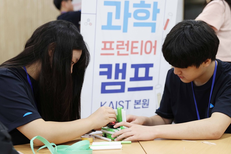 KAIST Holds '2025 KAIST Science Frontier Camp' for Multicultural Youth
<2025 KAIST Science Frontier Camp Activities>
KAIST (President Kwang Hyung Lee) announced on the 18th of July that it hosted the '2025 KAIST Science Frontier Camp' for multicultural youth from the 15th for three days and two nights at the Creative Learning Building on its main campus in Daejeon.
This event was organized in accordance with the 'Multicultural Talent Nurturing Agreement' signed by KAIST and GS Caltex in 2024. It marks the first year of a mid-to-long-term project in which 100 million KRW in development funds will be contributed annually for four years. The Global Institute for Talented Education organized the camp, and approximately 30 middle school students from multicultural families affiliated with the 'Hanmaum Educational Volunteer Group' (Director, Honorary Professor Byung Kyu Choi), a mentoring and volunteer organization for multicultural students, participated.
The camp participants enjoyed developing their scientific thinking skills and problem-solving abilities, and broadening their understanding of STEM (Science, Technology, Engineering, and Mathematics) career paths through a variety of science activity programs, including: △'Black Box: Record the Egg's Last Moment!' △'Find the Best Strategy! Heuristic Algorithm Challenge' △'Future Society and AI, Finding Career Directions' △'Distance Dominates the World!' and △'Career Talk Concert.'
During the opening ceremony, Director Byung Kyu Choi delivered a congratulatory speech. Additionally, Yong Hyun Kim, Dean of Admissions at KAIST, gave a special lecture titled 'La La Land KAIST – A Story of Chasing the Dream of a Young Scientist,' sharing honest stories about careers and dreams as a scientist.
Gi Jung Yoo, a freshman from the Division of Undeclared Majors who participated in the camp as a student mentor, shared that he had a very meaningful time mentoring the participating students, who are future STEM hopefuls, sharing vivid experiences as well as insights on metric functions. He added his hope that more students would be given such opportunities.
< Students Actively Taking Part in the Camp Activities>
Si Jong Kwak, Director of the Global Institute for Talented Education, stated, "We hope this will be a practical way to help students foster their interest in science, learn the joy of discussion and communication, and design their future."
KAIST President Kwang Hyung Lee remarked, "This camp was a valuable opportunity for students from diverse cultural backgrounds to gain confidence through science and envision their future." He added, "KAIST will continue to dedicate efforts to nurturing multicultural talent and contribute to creating a sustainable society."
Since 2024, KAIST has introduced and selected multicultural students through its Equal Opportunity Admission track. Utilizing the development funds from GS Caltex, KAIST also established the 'GS Caltex Multicultural Excellence Scholarship Program.' Through this scholarship program, undergraduate students from multicultural families receive living expenses each semester, allowing them to focus more stably on their studies. As the number of applicants for the Equal Opportunity Admission track is increasing every year, more multicultural students are expected to benefit from scholarships in the future.
Additionally, in May, both organizations invited Ms. Si Si Wu Fong, a foreign employee at GS Caltex, to give a special lecture titled 'Working Life for Foreigners in Korea' to support foreign students' career exploration. Foreign students who attended the lecture reported positive feedback, stating that they gained practical career information and were motivated to pursue employment in STEM fields in Korea.
KAIST plans to continue strengthening its efforts to nurture multicultural talent, increase understanding of the upcoming multicultural society, and help spread social values.
<At the 2025 KAIST Science Frontier Camp>
2025.07.18 View 521
KAIST Holds '2025 KAIST Science Frontier Camp' for Multicultural Youth
<2025 KAIST Science Frontier Camp Activities>
KAIST (President Kwang Hyung Lee) announced on the 18th of July that it hosted the '2025 KAIST Science Frontier Camp' for multicultural youth from the 15th for three days and two nights at the Creative Learning Building on its main campus in Daejeon.
This event was organized in accordance with the 'Multicultural Talent Nurturing Agreement' signed by KAIST and GS Caltex in 2024. It marks the first year of a mid-to-long-term project in which 100 million KRW in development funds will be contributed annually for four years. The Global Institute for Talented Education organized the camp, and approximately 30 middle school students from multicultural families affiliated with the 'Hanmaum Educational Volunteer Group' (Director, Honorary Professor Byung Kyu Choi), a mentoring and volunteer organization for multicultural students, participated.
The camp participants enjoyed developing their scientific thinking skills and problem-solving abilities, and broadening their understanding of STEM (Science, Technology, Engineering, and Mathematics) career paths through a variety of science activity programs, including: △'Black Box: Record the Egg's Last Moment!' △'Find the Best Strategy! Heuristic Algorithm Challenge' △'Future Society and AI, Finding Career Directions' △'Distance Dominates the World!' and △'Career Talk Concert.'
During the opening ceremony, Director Byung Kyu Choi delivered a congratulatory speech. Additionally, Yong Hyun Kim, Dean of Admissions at KAIST, gave a special lecture titled 'La La Land KAIST – A Story of Chasing the Dream of a Young Scientist,' sharing honest stories about careers and dreams as a scientist.
Gi Jung Yoo, a freshman from the Division of Undeclared Majors who participated in the camp as a student mentor, shared that he had a very meaningful time mentoring the participating students, who are future STEM hopefuls, sharing vivid experiences as well as insights on metric functions. He added his hope that more students would be given such opportunities.
< Students Actively Taking Part in the Camp Activities>
Si Jong Kwak, Director of the Global Institute for Talented Education, stated, "We hope this will be a practical way to help students foster their interest in science, learn the joy of discussion and communication, and design their future."
KAIST President Kwang Hyung Lee remarked, "This camp was a valuable opportunity for students from diverse cultural backgrounds to gain confidence through science and envision their future." He added, "KAIST will continue to dedicate efforts to nurturing multicultural talent and contribute to creating a sustainable society."
Since 2024, KAIST has introduced and selected multicultural students through its Equal Opportunity Admission track. Utilizing the development funds from GS Caltex, KAIST also established the 'GS Caltex Multicultural Excellence Scholarship Program.' Through this scholarship program, undergraduate students from multicultural families receive living expenses each semester, allowing them to focus more stably on their studies. As the number of applicants for the Equal Opportunity Admission track is increasing every year, more multicultural students are expected to benefit from scholarships in the future.
Additionally, in May, both organizations invited Ms. Si Si Wu Fong, a foreign employee at GS Caltex, to give a special lecture titled 'Working Life for Foreigners in Korea' to support foreign students' career exploration. Foreign students who attended the lecture reported positive feedback, stating that they gained practical career information and were motivated to pursue employment in STEM fields in Korea.
KAIST plans to continue strengthening its efforts to nurture multicultural talent, increase understanding of the upcoming multicultural society, and help spread social values.
<At the 2025 KAIST Science Frontier Camp>
2025.07.18 View 521 -
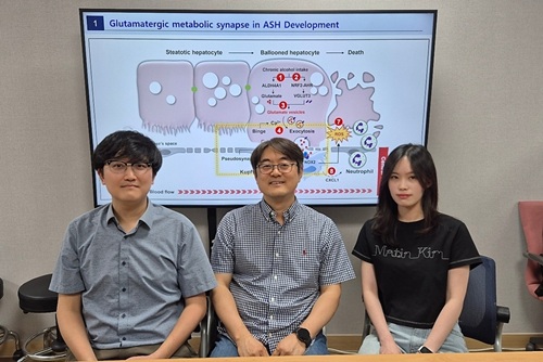 KAIST reveals for the first time the mechanism by which alcohol triggers liver inflammation
<(From left)Dr. Keungmo Yang, Professor Won-Il Jeong, Ph.D candidate Kyurae Kim>
Excessive alcohol consumption causes alcoholic liver disease, and about 20% of these cases progress to alcohol-associated steatohepatitis (ASH), which can lead to liver cirrhosis and liver failure. Early diagnosis and treatment are therefore extremely important. A KAIST research team has identified a new molecular mechanism in which alcohol-damaged liver cells increase reactive oxygen species (ROS), leading to cell death and inflammatory responses. In addition, they discovered that Kupffer cells, immune cells residing in the liver, act as a “dual-function regulator” that can either promote or suppress inflammation through interactions with liver cells.
KAIST (President Kwang-Hyung Lee) announced on the 17th that a research team led by Professor Won-Il Jeong from the Graduate School of Medical Science and Engineering, in collaboration with Professor Won Kim’s team at Seoul National University Boramae Medical Center, has uncovered the molecular pathway of liver damage and inflammation caused by alcohol consumption. This finding offers new clues for the diagnosis and treatment of alcohol-associated liver disease (ALD).
Professor Won-Il Jeong’s research team found that during chronic alcohol intake, expression of the vesicular glutamate transporter VGLUT3 increases, leading to glutamate accumulation in hepatocytes. Subsequent binge drinking causes rapid changes in intracellular calcium levels, which then triggers glutamate* secretion. The secreted glutamate stimulates the glutamate receptor mGluR5 on liver-resident macrophages (Kupffer cells), which induces ROS production and activates a pathological pathway resulting in hepatocyte death and inflammation.
*Glutamate: A type of amino acid involved in intercellular signaling, protein synthesis, and energy metabolism in various tissues including the brain and liver. In excess, it can cause overexcitation and death of nerve cells.
Glutamate accumulation in perivenous hepatocytes through vesicular glutamate transporter 3 after 2-week EtOH intake and its release by binge drinking>
A particularly groundbreaking aspect of this study is that damaged hepatocytes and Kupffer cells can form a "pseudosynapse"—a structure similar to a synapse which is previously thought to occur only in the brain—enabling them to exchange signals. This is the first time such a phenomenon has been identified in the liver.
This pseudosynapse forms when hepatocytes expand (ballooning) due to alcohol, becoming physically attached to Kupffer cells. Simply put, the damaged hepatocytes don’t just die—they send distress signals to nearby immune cells, prompting a response.
This discovery proposes a new paradigm: even in peripheral organs, direct structural contact between cells can allow signal transmission. It also shows that damaged hepatocytes can actively stimulate macrophages and induce regeneration through cell death, revealing the liver’s “autonomous recovery function.”
The team also confirmed in animal models that genetic or pharmacological inhibition of VGLUT3, mGluR5, or the ROS-producing enzyme NOX2 reduces alcohol-induced liver damage. They also confirmed that the same mechanism observed in animal models was present in human patients with ALD by analyzing blood and liver tissue samples.
Professor Won-Il Jeong of KAIST said, “These findings may serve as new molecular targets for early diagnosis and treatment of ASH in the future.”
This study was jointly led by Dr. Keungmo Yang (now at Yeouido St. Mary’s Hospital) and Kyurae Kim, a doctoral candidate at KAIST, who served as co–first authors. It was conducted in collaboration with Professor Won Kim’s team at Seoul National University Boramae Medical Center and was published in the journal Nature Communications on July 1.
※ Article Title: Binge drinking triggers VGLUT3-mediated glutamate secretion and subsequent hepatic inflammation by activating mGluR5/NOX2 in Kupffer cells ※ DOI: https://doi.org/10.1038/s41467-025-60820-3
This study was supported by the Ministry of Science and ICT through the National Research Foundation of Korea's Global Leader Program, Mid-Career Researcher Program, and the Bio & Medical Technology Development Program.
2025.07.17 View 646
KAIST reveals for the first time the mechanism by which alcohol triggers liver inflammation
<(From left)Dr. Keungmo Yang, Professor Won-Il Jeong, Ph.D candidate Kyurae Kim>
Excessive alcohol consumption causes alcoholic liver disease, and about 20% of these cases progress to alcohol-associated steatohepatitis (ASH), which can lead to liver cirrhosis and liver failure. Early diagnosis and treatment are therefore extremely important. A KAIST research team has identified a new molecular mechanism in which alcohol-damaged liver cells increase reactive oxygen species (ROS), leading to cell death and inflammatory responses. In addition, they discovered that Kupffer cells, immune cells residing in the liver, act as a “dual-function regulator” that can either promote or suppress inflammation through interactions with liver cells.
KAIST (President Kwang-Hyung Lee) announced on the 17th that a research team led by Professor Won-Il Jeong from the Graduate School of Medical Science and Engineering, in collaboration with Professor Won Kim’s team at Seoul National University Boramae Medical Center, has uncovered the molecular pathway of liver damage and inflammation caused by alcohol consumption. This finding offers new clues for the diagnosis and treatment of alcohol-associated liver disease (ALD).
Professor Won-Il Jeong’s research team found that during chronic alcohol intake, expression of the vesicular glutamate transporter VGLUT3 increases, leading to glutamate accumulation in hepatocytes. Subsequent binge drinking causes rapid changes in intracellular calcium levels, which then triggers glutamate* secretion. The secreted glutamate stimulates the glutamate receptor mGluR5 on liver-resident macrophages (Kupffer cells), which induces ROS production and activates a pathological pathway resulting in hepatocyte death and inflammation.
*Glutamate: A type of amino acid involved in intercellular signaling, protein synthesis, and energy metabolism in various tissues including the brain and liver. In excess, it can cause overexcitation and death of nerve cells.
Glutamate accumulation in perivenous hepatocytes through vesicular glutamate transporter 3 after 2-week EtOH intake and its release by binge drinking>
A particularly groundbreaking aspect of this study is that damaged hepatocytes and Kupffer cells can form a "pseudosynapse"—a structure similar to a synapse which is previously thought to occur only in the brain—enabling them to exchange signals. This is the first time such a phenomenon has been identified in the liver.
This pseudosynapse forms when hepatocytes expand (ballooning) due to alcohol, becoming physically attached to Kupffer cells. Simply put, the damaged hepatocytes don’t just die—they send distress signals to nearby immune cells, prompting a response.
This discovery proposes a new paradigm: even in peripheral organs, direct structural contact between cells can allow signal transmission. It also shows that damaged hepatocytes can actively stimulate macrophages and induce regeneration through cell death, revealing the liver’s “autonomous recovery function.”
The team also confirmed in animal models that genetic or pharmacological inhibition of VGLUT3, mGluR5, or the ROS-producing enzyme NOX2 reduces alcohol-induced liver damage. They also confirmed that the same mechanism observed in animal models was present in human patients with ALD by analyzing blood and liver tissue samples.
Professor Won-Il Jeong of KAIST said, “These findings may serve as new molecular targets for early diagnosis and treatment of ASH in the future.”
This study was jointly led by Dr. Keungmo Yang (now at Yeouido St. Mary’s Hospital) and Kyurae Kim, a doctoral candidate at KAIST, who served as co–first authors. It was conducted in collaboration with Professor Won Kim’s team at Seoul National University Boramae Medical Center and was published in the journal Nature Communications on July 1.
※ Article Title: Binge drinking triggers VGLUT3-mediated glutamate secretion and subsequent hepatic inflammation by activating mGluR5/NOX2 in Kupffer cells ※ DOI: https://doi.org/10.1038/s41467-025-60820-3
This study was supported by the Ministry of Science and ICT through the National Research Foundation of Korea's Global Leader Program, Mid-Career Researcher Program, and the Bio & Medical Technology Development Program.
2025.07.17 View 646 -
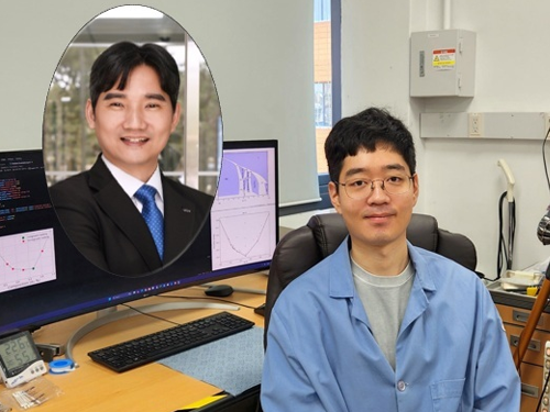 KAIST Ushers in Era of Predicting ‘Optimal Alloys’ Using AI, Without High-Temperature Experiments
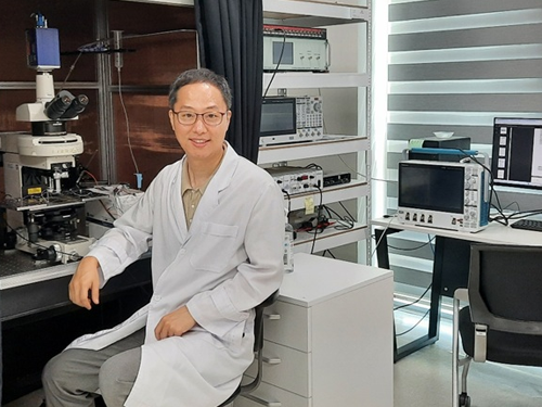
<Picture1.(From Left) Prof. Seungbum Hong, Ph.D candidate Youngwoo Choi>
Steel alloys used in automobiles and machinery parts are typically manufactured through a melting process at high temperatures. The phenomenon where the components remain unchanged during melting is called “congruent melting.” KAIST researchers have now addressed this process—traditionally only possible through high-temperature experiments—using artificial intelligence (AI). This study draws attention as it proposes a new direction for future alloy development by predicting in advance how well alloy components will mix during melting, a long-standing challenge in the field.
KAIST (President Kwang Hyung Lee) announced on the 14th of July that Professor Seungbum Hong’s research team from the Department of Materials Science and Engineering, in international collaboration with Professor Chris Wolverton’s group at Northwestern University, has developed a high-accuracy machine learning model that predicts whether alloy components will remain stable during melting. This was achieved using formation energy data derived from Density Functional Theory (DFT)* calculations.
*Density Functional Theory (DFT): A computational quantum mechanical method used to investigate the electronic structure of many-body systems, especially atoms, molecules, and solids, based on electron density.
The research team combined formation energy values obtained via DFT with experimental melting reaction data to train a machine learning model on 4,536 binary compounds.
Among the various machine learning algorithms tested, the XGBoost-based classification model demonstrated the highest accuracy in predicting whether alloys would mix well, achieving a prediction accuracy of approximately 82.5%. The team also applied the Shapley value method* to analyze the key features of the model. One major finding was that sharp changes in the slope of the formation energy curve (referred to as “convex hull sharpness”) were the most significant factor. A steep slope indicates a composition with energetically favorable (i.e., stable) formation.
*Shapley value: An explainability method in AI used to determine how much each feature contributed to a prediction.
The most notable significance of this study is that it predicts alloy melting behavior without performing high-temperature experiments. This is especially useful for materials such as high-entropy alloys or ultra-heat-resistant alloys, which are difficult to handle experimentally. The approach could also be extended to the design of complex multi-component alloy systems in the future.
Furthermore, the physical indicators identified by the AI model showed high consistency with actual experimental results on how well alloys mix and remain stable. This suggests that the model could be broadly applied to the development of various metal materials and the prediction of structural stability.
Professor Seungbum Hong of KAIST stated, “This research demonstrates how data-driven predictive materials development is possible by integrating computational methods, experimental data, and machine learning—departing from the traditional experience-based alloy design.” He added, “In the future, by incorporating state-of-the-art AI techniques such as generative models and reinforcement learning, we could enter an era where completely new alloys are designed automatically.”
<Model performance and feature importance analysis for predicting melting congruency. (a) SHAP summary plot showing the impact of individual features on model predictions. (b) Confusion matrix illustrating the model’s classification performance. (c) Receiver operating characteristic (ROC) curve with an AUC (area under the curve) score of 0.87, indicating a strong classification performance.>
Ph.D. candidate Youngwoo Choi, from the Department of Materials Science and Engineering at KAIST, participated as the first author. The study was published in the May issue of APL Machine Learning, a prestigious journal in the field of machine learning published by the American Institute of Physics, and was selected as a “Featured Article.”
※ Paper title: Machine learning-based melting congruency prediction of binary compounds using density functional theory-calculated formation energy ※ DOI: 10.1063/5.0247514
This research was supported by the Ministry of Science and ICT and the National Research Foundation of Korea.
2025.07.14 View 470
KAIST Ushers in Era of Predicting ‘Optimal Alloys’ Using AI, Without High-Temperature Experiments
<Picture1.(From Left) Prof. Seungbum Hong, Ph.D candidate Youngwoo Choi>
Steel alloys used in automobiles and machinery parts are typically manufactured through a melting process at high temperatures. The phenomenon where the components remain unchanged during melting is called “congruent melting.” KAIST researchers have now addressed this process—traditionally only possible through high-temperature experiments—using artificial intelligence (AI). This study draws attention as it proposes a new direction for future alloy development by predicting in advance how well alloy components will mix during melting, a long-standing challenge in the field.
KAIST (President Kwang Hyung Lee) announced on the 14th of July that Professor Seungbum Hong’s research team from the Department of Materials Science and Engineering, in international collaboration with Professor Chris Wolverton’s group at Northwestern University, has developed a high-accuracy machine learning model that predicts whether alloy components will remain stable during melting. This was achieved using formation energy data derived from Density Functional Theory (DFT)* calculations.
*Density Functional Theory (DFT): A computational quantum mechanical method used to investigate the electronic structure of many-body systems, especially atoms, molecules, and solids, based on electron density.
The research team combined formation energy values obtained via DFT with experimental melting reaction data to train a machine learning model on 4,536 binary compounds.
Among the various machine learning algorithms tested, the XGBoost-based classification model demonstrated the highest accuracy in predicting whether alloys would mix well, achieving a prediction accuracy of approximately 82.5%. The team also applied the Shapley value method* to analyze the key features of the model. One major finding was that sharp changes in the slope of the formation energy curve (referred to as “convex hull sharpness”) were the most significant factor. A steep slope indicates a composition with energetically favorable (i.e., stable) formation.
*Shapley value: An explainability method in AI used to determine how much each feature contributed to a prediction.
The most notable significance of this study is that it predicts alloy melting behavior without performing high-temperature experiments. This is especially useful for materials such as high-entropy alloys or ultra-heat-resistant alloys, which are difficult to handle experimentally. The approach could also be extended to the design of complex multi-component alloy systems in the future.
Furthermore, the physical indicators identified by the AI model showed high consistency with actual experimental results on how well alloys mix and remain stable. This suggests that the model could be broadly applied to the development of various metal materials and the prediction of structural stability.
Professor Seungbum Hong of KAIST stated, “This research demonstrates how data-driven predictive materials development is possible by integrating computational methods, experimental data, and machine learning—departing from the traditional experience-based alloy design.” He added, “In the future, by incorporating state-of-the-art AI techniques such as generative models and reinforcement learning, we could enter an era where completely new alloys are designed automatically.”
<Model performance and feature importance analysis for predicting melting congruency. (a) SHAP summary plot showing the impact of individual features on model predictions. (b) Confusion matrix illustrating the model’s classification performance. (c) Receiver operating characteristic (ROC) curve with an AUC (area under the curve) score of 0.87, indicating a strong classification performance.>
Ph.D. candidate Youngwoo Choi, from the Department of Materials Science and Engineering at KAIST, participated as the first author. The study was published in the May issue of APL Machine Learning, a prestigious journal in the field of machine learning published by the American Institute of Physics, and was selected as a “Featured Article.”
※ Paper title: Machine learning-based melting congruency prediction of binary compounds using density functional theory-calculated formation energy ※ DOI: 10.1063/5.0247514
This research was supported by the Ministry of Science and ICT and the National Research Foundation of Korea.
2025.07.14 View 470 -
 KAIST Shows That the Brain Can Distinguish Glucose: Clues to Treat Obesity and Diabetes
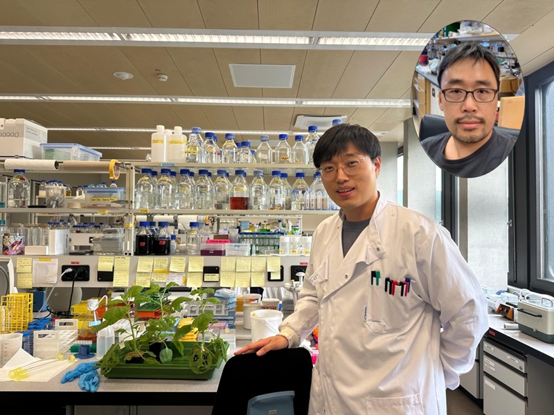
<(From left)Prof. Greg S.B Suh, Dr. Jieun Kim, Dr. Shinhye Kim, Researcher Wongyo Jeong)
“How does our brain distinguish glucose from the many nutrients absorbed in the gut?” Starting with this question, a KAIST research team has demonstrated that the brain can selectively recognize specific nutrients—particularly glucose—beyond simply detecting total calorie content. This study is expected to offer a new paradigm for appetite control and the treatment of metabolic diseases.
On the 9th, KAIST (President Kwang Hyung Lee) announced that Professor Greg S.B. Suh’s team in the Department of Biological Sciences, in collaboration with Professor Young-Gyun Park’s team (BarNeuro), Professor Seung-Hee Lee’s team (Department of Biological Sciences), and the Albert Einstein College of Medicine in New York, had identified the existence of a gut-brain circuit that allows animals in a hungry state to selectively detect and prefer glucose in the gut.
Organisms derive energy from various nutrients including sugars, proteins, and fats. Previous studies have shown that total caloric information in the gut suppresses hunger neurons in the hypothalamus to regulate appetite. However, the existence of a gut-brain circuit that specifically responds to glucose and corresponding brain cells had not been demonstrated until now.
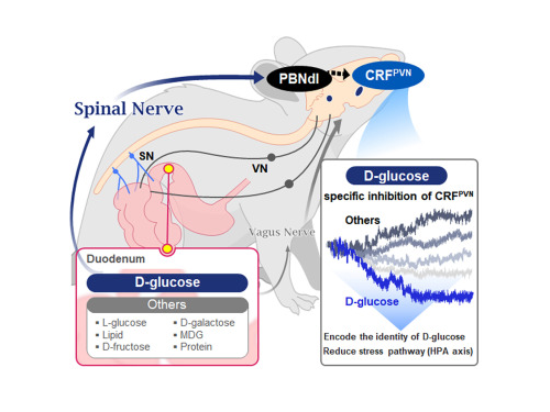
In this study, the team successfully identified a “gut-brain circuit” that senses glucose—essential for brain function—and regulates food intake behavior for required nutrients.
They further proved, for the first time, that this circuit responds within seconds to not only hunger or external stimuli but also to specific caloric nutrients directly introduced into the small intestine, particularly D-glucose, through the activity of “CRF neurons*” in the brain’s hypothalamus.
*CRF neurons: These neurons secrete corticotropin-releasing factor (CRF) in the hypothalamus and are central to the hypothalamic-pituitary-adrenal (HPA) axis, the body’s core physiological system for responding to stress. CRF neurons are known to regulate neuroendocrine balance in response to stress stimuli.
Using optogenetics to precisely track neural activity in real time, the researchers injected various nutrients—D-glucose, L-glucose, amino acids, and fats—directly into the small intestines of mice and observed the results.
They discovered that among the CRF neurons located in the paraventricular nucleus (PVN)* of the hypothalamus, only those specific to D-glucose showed selective responses. These neurons did not respond—or showed inverse reactions—to other sugars or to proteins and fats. This is the first demonstration that single neurons in the brain can guide nutrient-specific responses depending on gut nutrient influx.
*PVN (Paraventricular Nucleus): A key nucleus within the hypothalamus responsible for maintaining bodily homeostasis.
The team also revealed that glucose-sensing signals in the small intestine are transmitted via the spinal cord to the dorsolateral parabrachial nucleus (PBNdl) of the brain, and from there to CRF neurons in the PVN. In contrast, signals for amino acids and fats are transmitted to the brain through the vagus nerve, a different pathway.
In optogenetic inhibition experiments, suppressing CRF neurons in fasting mice eliminated their preference for glucose, proving that this circuit is essential for glucose-specific nutrient preference.
This study was inspired by Professor Suh’s earlier research at NYU using fruit flies, where he identified “DH44 neurons” that selectively detect glucose and sugar in the gut. Based on the hypothesis that hypothalamic neurons in mammals would show similar functional responses to glucose, the current study was launched.
To test this hypothesis, Dr. Jineun Kim (KAIST Ph.D. graduate, now at Caltech) demonstrated during her doctoral research that hungry mice preferred glucose among various intragastrically infused nutrients and that CRF neurons exhibited rapid and specific responses.
Along with Wongyo Jung (KAIST B.S. graduate, now Ph.D. student at Caltech), they modeled and experimentally confirmed the critical role of CRF neurons. Dr. Shinhye Kim, through collaboration, revealed that specific spinal neurons play a key role in conveying intestinal nutrient information to the brain.
Dr. Jineun Kim and Dr. Shinhye Kim said, “This study started from a simple but fundamental question—‘How does the brain distinguish glucose from various nutrients absorbed in the gut?’ We have shown that spinal-based gut-brain circuits play a central role in energy metabolism and homeostasis by transmitting specific gut nutrient signals to the brain.”
Professor Suh added, “By identifying a gut-brain pathway specialized for glucose, this research offers a new therapeutic target for metabolic diseases such as obesity and diabetes. Our future research will explore similar circuits for sensing other essential nutrients like amino acids and fats and their interaction mechanisms.”
Ph.D. student Jineun Kim, Dr. Shinhye Kim, and student Wongyo Jung (co-first authors) contributed to this study, which was published online in the international journal Neuron on June 20, 2025.
※ Paper Title: Encoding the glucose identity by discrete hypothalamic neurons via the gut-brain axis ※ DOI: https://doi.org/10.1016/j.neuron.2025.05.024
This study was supported by the Samsung Science & Technology Foundation, the National Research Foundation of Korea (NRF) Leader Research Program, the POSCO Cheongam Science Fellowship, the Asan Foundation Biomedical Science Scholarship, the Institute for Basic Science (IBS), and the KAIST KAIX program.
2025.07.09 View 766
KAIST Shows That the Brain Can Distinguish Glucose: Clues to Treat Obesity and Diabetes
<(From left)Prof. Greg S.B Suh, Dr. Jieun Kim, Dr. Shinhye Kim, Researcher Wongyo Jeong)
“How does our brain distinguish glucose from the many nutrients absorbed in the gut?” Starting with this question, a KAIST research team has demonstrated that the brain can selectively recognize specific nutrients—particularly glucose—beyond simply detecting total calorie content. This study is expected to offer a new paradigm for appetite control and the treatment of metabolic diseases.
On the 9th, KAIST (President Kwang Hyung Lee) announced that Professor Greg S.B. Suh’s team in the Department of Biological Sciences, in collaboration with Professor Young-Gyun Park’s team (BarNeuro), Professor Seung-Hee Lee’s team (Department of Biological Sciences), and the Albert Einstein College of Medicine in New York, had identified the existence of a gut-brain circuit that allows animals in a hungry state to selectively detect and prefer glucose in the gut.
Organisms derive energy from various nutrients including sugars, proteins, and fats. Previous studies have shown that total caloric information in the gut suppresses hunger neurons in the hypothalamus to regulate appetite. However, the existence of a gut-brain circuit that specifically responds to glucose and corresponding brain cells had not been demonstrated until now.
In this study, the team successfully identified a “gut-brain circuit” that senses glucose—essential for brain function—and regulates food intake behavior for required nutrients.
They further proved, for the first time, that this circuit responds within seconds to not only hunger or external stimuli but also to specific caloric nutrients directly introduced into the small intestine, particularly D-glucose, through the activity of “CRF neurons*” in the brain’s hypothalamus.
*CRF neurons: These neurons secrete corticotropin-releasing factor (CRF) in the hypothalamus and are central to the hypothalamic-pituitary-adrenal (HPA) axis, the body’s core physiological system for responding to stress. CRF neurons are known to regulate neuroendocrine balance in response to stress stimuli.
Using optogenetics to precisely track neural activity in real time, the researchers injected various nutrients—D-glucose, L-glucose, amino acids, and fats—directly into the small intestines of mice and observed the results.
They discovered that among the CRF neurons located in the paraventricular nucleus (PVN)* of the hypothalamus, only those specific to D-glucose showed selective responses. These neurons did not respond—or showed inverse reactions—to other sugars or to proteins and fats. This is the first demonstration that single neurons in the brain can guide nutrient-specific responses depending on gut nutrient influx.
*PVN (Paraventricular Nucleus): A key nucleus within the hypothalamus responsible for maintaining bodily homeostasis.
The team also revealed that glucose-sensing signals in the small intestine are transmitted via the spinal cord to the dorsolateral parabrachial nucleus (PBNdl) of the brain, and from there to CRF neurons in the PVN. In contrast, signals for amino acids and fats are transmitted to the brain through the vagus nerve, a different pathway.
In optogenetic inhibition experiments, suppressing CRF neurons in fasting mice eliminated their preference for glucose, proving that this circuit is essential for glucose-specific nutrient preference.
This study was inspired by Professor Suh’s earlier research at NYU using fruit flies, where he identified “DH44 neurons” that selectively detect glucose and sugar in the gut. Based on the hypothesis that hypothalamic neurons in mammals would show similar functional responses to glucose, the current study was launched.
To test this hypothesis, Dr. Jineun Kim (KAIST Ph.D. graduate, now at Caltech) demonstrated during her doctoral research that hungry mice preferred glucose among various intragastrically infused nutrients and that CRF neurons exhibited rapid and specific responses.
Along with Wongyo Jung (KAIST B.S. graduate, now Ph.D. student at Caltech), they modeled and experimentally confirmed the critical role of CRF neurons. Dr. Shinhye Kim, through collaboration, revealed that specific spinal neurons play a key role in conveying intestinal nutrient information to the brain.
Dr. Jineun Kim and Dr. Shinhye Kim said, “This study started from a simple but fundamental question—‘How does the brain distinguish glucose from various nutrients absorbed in the gut?’ We have shown that spinal-based gut-brain circuits play a central role in energy metabolism and homeostasis by transmitting specific gut nutrient signals to the brain.”
Professor Suh added, “By identifying a gut-brain pathway specialized for glucose, this research offers a new therapeutic target for metabolic diseases such as obesity and diabetes. Our future research will explore similar circuits for sensing other essential nutrients like amino acids and fats and their interaction mechanisms.”
Ph.D. student Jineun Kim, Dr. Shinhye Kim, and student Wongyo Jung (co-first authors) contributed to this study, which was published online in the international journal Neuron on June 20, 2025.
※ Paper Title: Encoding the glucose identity by discrete hypothalamic neurons via the gut-brain axis ※ DOI: https://doi.org/10.1016/j.neuron.2025.05.024
This study was supported by the Samsung Science & Technology Foundation, the National Research Foundation of Korea (NRF) Leader Research Program, the POSCO Cheongam Science Fellowship, the Asan Foundation Biomedical Science Scholarship, the Institute for Basic Science (IBS), and the KAIST KAIX program.
2025.07.09 View 766 -
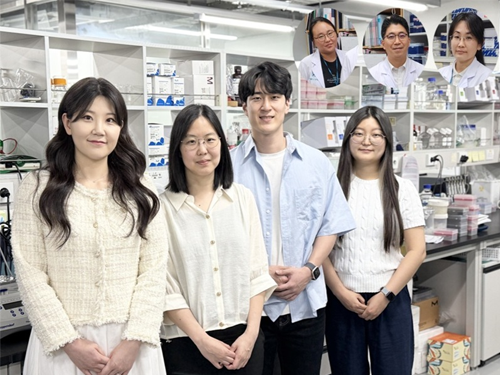 KAIST Develops Novel Candidiasis Treatment Overcoming Side Effects and Resistance
<(From left) Ph. D Candidate Ju Yeon Chung, Prof.Hyun Jung Chung, Ph.D candidate Seungju Yang, Ph.D candidate Ayoung Park, Dr. Yoon-Kyoung Hong from Asan Medical Center, Prof. Yong Pil Chong, Dr. Eunhee Jeon>
Candida, a type of fungus, which can spread throughout the body via the bloodstream, leading to organ damage and sepsis. Recently, the incidence of candidiasis has surged due to the increase in immunosuppressive therapies, medical implants, and transplantation. Korean researchers have successfully developed a next-generation treatment that, unlike existing antifungals, selectively acts only on Candida, achieving both high therapeutic efficacy and low side effects simultaneously.
KAIST (President Kwang Hyung Lee) announced on the 8th that a research team led by Professor Hyun-Jung Chung of the Department of Biological Sciences, in collaboration with Professor Yong Pil Jeong's team at Asan Medical Center, developed a gene-based nanotherapy (FTNx) that simultaneously inhibits two key enzymes in the Candida cell wall.
Current antifungal drugs for Candida have low target selectivity, which can affect human cells. Furthermore, their therapeutic efficacy is gradually decreasing due to the emergence of new resistant strains. Especially for immunocompromised patients, the infection progresses rapidly and has a poor prognosis, making the development of new treatments to overcome the limitations of existing therapies urgent.
The developed treatment can be administered systemically, and by combining gene suppression technology with nanomaterial technology, it effectively overcomes the structural limitations of existing compound-based drugs and successfully achieves selective treatment against only Candida.
The research team created a gold nanoparticle-based complex loaded with short DNA fragments called antisense oligonucleotides (ASO), which simultaneously target two crucial enzymes—β-1,3-glucan synthase (FKS1) and chitin synthase (CHS3)—important for forming the cell wall of the Candida fungus.
By applying a surface coating technology that binds to a specific glycolipid structure (a structure combining sugar and fat) on the Candida cell wall, a targeted delivery device was implemented. This successfully achieved a precise targeting effect, ensuring the complex is not delivered to human cells at all but acts selectively only on Candida.
<Figure 1: Overview of antifungal therapy design and experimental approach>
This complex, after entering Candida cells, cleaves the mRNA produced by the FKS1 and CHS3 genes, thereby inhibiting translation and simultaneously blocking the synthesis of cell wall components β-1,3-glucan and chitin. As a result, the
Candida cell wall loses its structural stability and collapses, suppressing bacterial survival and proliferation.
In fact, experiments using a systemic candidiasis model in mice confirmed the therapeutic effect: a significant reduction in
Candida count in the organs, normalization of immune responses, and a notable increase in survival rates were observed in the treated group.
Professor Hyun-Jung Chung, who led the research, stated, "This study presents a method to overcome the issues of human toxicity and drug resistance spread with existing treatments, marking an important turning point by demonstrating the applicability of gene therapy for systemic infections". She added, "We plan to continue research on optimizing administration methods and verifying toxicity for future clinical application."
This research involved Ju Yeon Chung and Yoon-Kyoung Hong as co-first authors , and was published in the international journal 'Nature Communications' on July 1st.
Paper Title: Effective treatment of systemic candidiasis by synergistic targeting of cell wall synthesis
DOI: 10.1038/s41467-025-60684-7
This research was supported by the Ministry of Health and Welfare and the National Research Foundation of Korea.
2025.07.08 View 708
KAIST Develops Novel Candidiasis Treatment Overcoming Side Effects and Resistance
<(From left) Ph. D Candidate Ju Yeon Chung, Prof.Hyun Jung Chung, Ph.D candidate Seungju Yang, Ph.D candidate Ayoung Park, Dr. Yoon-Kyoung Hong from Asan Medical Center, Prof. Yong Pil Chong, Dr. Eunhee Jeon>
Candida, a type of fungus, which can spread throughout the body via the bloodstream, leading to organ damage and sepsis. Recently, the incidence of candidiasis has surged due to the increase in immunosuppressive therapies, medical implants, and transplantation. Korean researchers have successfully developed a next-generation treatment that, unlike existing antifungals, selectively acts only on Candida, achieving both high therapeutic efficacy and low side effects simultaneously.
KAIST (President Kwang Hyung Lee) announced on the 8th that a research team led by Professor Hyun-Jung Chung of the Department of Biological Sciences, in collaboration with Professor Yong Pil Jeong's team at Asan Medical Center, developed a gene-based nanotherapy (FTNx) that simultaneously inhibits two key enzymes in the Candida cell wall.
Current antifungal drugs for Candida have low target selectivity, which can affect human cells. Furthermore, their therapeutic efficacy is gradually decreasing due to the emergence of new resistant strains. Especially for immunocompromised patients, the infection progresses rapidly and has a poor prognosis, making the development of new treatments to overcome the limitations of existing therapies urgent.
The developed treatment can be administered systemically, and by combining gene suppression technology with nanomaterial technology, it effectively overcomes the structural limitations of existing compound-based drugs and successfully achieves selective treatment against only Candida.
The research team created a gold nanoparticle-based complex loaded with short DNA fragments called antisense oligonucleotides (ASO), which simultaneously target two crucial enzymes—β-1,3-glucan synthase (FKS1) and chitin synthase (CHS3)—important for forming the cell wall of the Candida fungus.
By applying a surface coating technology that binds to a specific glycolipid structure (a structure combining sugar and fat) on the Candida cell wall, a targeted delivery device was implemented. This successfully achieved a precise targeting effect, ensuring the complex is not delivered to human cells at all but acts selectively only on Candida.
<Figure 1: Overview of antifungal therapy design and experimental approach>
This complex, after entering Candida cells, cleaves the mRNA produced by the FKS1 and CHS3 genes, thereby inhibiting translation and simultaneously blocking the synthesis of cell wall components β-1,3-glucan and chitin. As a result, the
Candida cell wall loses its structural stability and collapses, suppressing bacterial survival and proliferation.
In fact, experiments using a systemic candidiasis model in mice confirmed the therapeutic effect: a significant reduction in
Candida count in the organs, normalization of immune responses, and a notable increase in survival rates were observed in the treated group.
Professor Hyun-Jung Chung, who led the research, stated, "This study presents a method to overcome the issues of human toxicity and drug resistance spread with existing treatments, marking an important turning point by demonstrating the applicability of gene therapy for systemic infections". She added, "We plan to continue research on optimizing administration methods and verifying toxicity for future clinical application."
This research involved Ju Yeon Chung and Yoon-Kyoung Hong as co-first authors , and was published in the international journal 'Nature Communications' on July 1st.
Paper Title: Effective treatment of systemic candidiasis by synergistic targeting of cell wall synthesis
DOI: 10.1038/s41467-025-60684-7
This research was supported by the Ministry of Health and Welfare and the National Research Foundation of Korea.
2025.07.08 View 708 -
 KAIST Presents a Breakthrough in Overcoming Drug Resistance in Cancer – Hope for Treating Intractable Diseases like Diabetes
<(From the left) Prof. Hyun Uk Kim, Ph.D candiate Hae Deok Jung, Ph.D candidate Jina Lim, Prof.Yoosik Kim from the Department of Chemical and Biomolecular Engineering>
One of the biggest obstacles in cancer treatment is drug resistance in cancer cells. Conventional efforts have focused on identifying new drug targets to eliminate these resistant cells, but such approaches can often lead to even stronger resistance. Now, researchers at KAIST have developed a computational framework to predict key metabolic genes that can re-sensitize resistant cancer cells to treatment. This technique holds promise not only for a variety of cancer therapies but also for treating metabolic diseases such as diabetes.
On the 7th of July, KAIST (President Kwang Hyung Lee) announced that a research team led by Professors Hyun Uk Kim and Yoosik Kim from the Department of Chemical and Biomolecular Engineering had developed a computational framework that predicts metabolic gene targets to re-sensitize drug-resistant breast cancer cells. This was achieved using a metabolic network model capable of simulating human metabolism.
Focusing on metabolic alterations—key characteristics in the formation of drug resistance—the researchers developed a metabolism-based approach to identify gene targets that could enhance drug responsiveness by regulating the metabolism of drug-resistant breast cancer cells.
< Computational framework that can identify metabolic gene targets to revert the metabolic state of the drug-resistant cells to that of the drug-sensitive parental cells>
The team first constructed cell-specific metabolic network models by integrating proteomic data obtained from two different types of drug-resistant MCF7 breast cancer cell lines: one resistant to doxorubicin and the other to paclitaxel. They then performed gene knockout simulations* on all of the metabolic genes and analyzed the results.
*Gene knockout simulation: A computational method to predict changes in a biological network by virtually removing specific genes.
As a result, they discovered that suppressing certain genes could make previously resistant cancer cells responsive to anticancer drugs again. Specifically, they identified GOT1 as a target in doxorubicin-resistant cells, GPI in paclitaxel-resistant cells, and SLC1A5 as a common target for both drugs.
The predictions were experimentally validated by suppressing proteins encoded by these genes, which led to the re-sensitization of the drug-resistant cancer cells.
Furthermore, consistent re-sensitization effects were also observed when the same proteins were inhibited in other types of breast cancer cells that had developed resistance to the same drugs.
Professor Yoosik Kim remarked, “Cellular metabolism plays a crucial role in various intractable diseases including infectious and degenerative conditions. This new technology, which predicts metabolic regulation switches, can serve as a foundational tool not only for treating drug-resistant breast cancer but also for a wide range of diseases that currently lack effective therapies.”
Professor Hyun Uk Kim, who led the study, emphasized, “The significance of this research lies in our ability to accurately predict key metabolic genes that can make resistant cancer cells responsive to treatment again—using only computer simulations and minimal experimental data. This framework can be widely applied to discover new therapeutic targets in various cancers and metabolic diseases.”
The study, in which Ph.D. candidates JinA Lim and Hae Deok Jung from KAIST participated as co-first authors, was published online on June 25 in Proceedings of the National Academy of Sciences (PNAS), a leading multidisciplinary journal that covers top-tier research in life sciences, physics, engineering, and social sciences.
※ Title: Genome-scale knockout simulation and clustering analysis of drug-resistant breast cancer cells reveal drug sensitization targets ※ DOI: https://doi.org/10.1073/pnas.2425384122 ※ Authors: JinA Lim (KAIST, co-first author), Hae Deok Jung (KAIST, co-first author), Han Suk Ryu (Seoul National University Hospital, corresponding author), Yoosik Kim (KAIST, corresponding author), Hyun Uk Kim (KAIST, corresponding author), and five others.
This research was supported by the Ministry of Science and ICT through the National Research Foundation of Korea, and the Electronics and Telecommunications Research Institute (ETRI).
2025.07.08 View 1149
KAIST Presents a Breakthrough in Overcoming Drug Resistance in Cancer – Hope for Treating Intractable Diseases like Diabetes
<(From the left) Prof. Hyun Uk Kim, Ph.D candiate Hae Deok Jung, Ph.D candidate Jina Lim, Prof.Yoosik Kim from the Department of Chemical and Biomolecular Engineering>
One of the biggest obstacles in cancer treatment is drug resistance in cancer cells. Conventional efforts have focused on identifying new drug targets to eliminate these resistant cells, but such approaches can often lead to even stronger resistance. Now, researchers at KAIST have developed a computational framework to predict key metabolic genes that can re-sensitize resistant cancer cells to treatment. This technique holds promise not only for a variety of cancer therapies but also for treating metabolic diseases such as diabetes.
On the 7th of July, KAIST (President Kwang Hyung Lee) announced that a research team led by Professors Hyun Uk Kim and Yoosik Kim from the Department of Chemical and Biomolecular Engineering had developed a computational framework that predicts metabolic gene targets to re-sensitize drug-resistant breast cancer cells. This was achieved using a metabolic network model capable of simulating human metabolism.
Focusing on metabolic alterations—key characteristics in the formation of drug resistance—the researchers developed a metabolism-based approach to identify gene targets that could enhance drug responsiveness by regulating the metabolism of drug-resistant breast cancer cells.
< Computational framework that can identify metabolic gene targets to revert the metabolic state of the drug-resistant cells to that of the drug-sensitive parental cells>
The team first constructed cell-specific metabolic network models by integrating proteomic data obtained from two different types of drug-resistant MCF7 breast cancer cell lines: one resistant to doxorubicin and the other to paclitaxel. They then performed gene knockout simulations* on all of the metabolic genes and analyzed the results.
*Gene knockout simulation: A computational method to predict changes in a biological network by virtually removing specific genes.
As a result, they discovered that suppressing certain genes could make previously resistant cancer cells responsive to anticancer drugs again. Specifically, they identified GOT1 as a target in doxorubicin-resistant cells, GPI in paclitaxel-resistant cells, and SLC1A5 as a common target for both drugs.
The predictions were experimentally validated by suppressing proteins encoded by these genes, which led to the re-sensitization of the drug-resistant cancer cells.
Furthermore, consistent re-sensitization effects were also observed when the same proteins were inhibited in other types of breast cancer cells that had developed resistance to the same drugs.
Professor Yoosik Kim remarked, “Cellular metabolism plays a crucial role in various intractable diseases including infectious and degenerative conditions. This new technology, which predicts metabolic regulation switches, can serve as a foundational tool not only for treating drug-resistant breast cancer but also for a wide range of diseases that currently lack effective therapies.”
Professor Hyun Uk Kim, who led the study, emphasized, “The significance of this research lies in our ability to accurately predict key metabolic genes that can make resistant cancer cells responsive to treatment again—using only computer simulations and minimal experimental data. This framework can be widely applied to discover new therapeutic targets in various cancers and metabolic diseases.”
The study, in which Ph.D. candidates JinA Lim and Hae Deok Jung from KAIST participated as co-first authors, was published online on June 25 in Proceedings of the National Academy of Sciences (PNAS), a leading multidisciplinary journal that covers top-tier research in life sciences, physics, engineering, and social sciences.
※ Title: Genome-scale knockout simulation and clustering analysis of drug-resistant breast cancer cells reveal drug sensitization targets ※ DOI: https://doi.org/10.1073/pnas.2425384122 ※ Authors: JinA Lim (KAIST, co-first author), Hae Deok Jung (KAIST, co-first author), Han Suk Ryu (Seoul National University Hospital, corresponding author), Yoosik Kim (KAIST, corresponding author), Hyun Uk Kim (KAIST, corresponding author), and five others.
This research was supported by the Ministry of Science and ICT through the National Research Foundation of Korea, and the Electronics and Telecommunications Research Institute (ETRI).
2025.07.08 View 1149 -
 Professor Moon-Jeong Choi Appointed as an Advisor for the ITU's 'AI for Good Global Summit'
Professor Moon-Jeong Choi from KAIST’s Graduate School of Science and Technology Policy has been appointed as an advisor for "Innovate for Impact" at the AI for Good Global Summit, organized by the International Telecommunication Union (ITU), a specialized agency of the United Nations (UN).
The ITU is the UN's oldest specialized agency in the field of information and communication technology (ICT) and serves as a crucial body for coordinating global ICT policies and standards.
This advisory committee was formed to explore global cooperation strategies for realizing the social value of Artificial Intelligence (AI) and promoting sustainable development. Experts from around the world are participating as committee members, with Professor Choi being the sole Korean representative.
<Moon-Jeong Choi from KAIST’s Graduate School of Science and Technology Policy>
The AI for Good Global Summit is taking place in Geneva, Switzerland from July 8 to 11. It is organized by the ITU in collaboration with approximately 40 other UN-affiliated organizations. The summit aims to address global challenges facing humanity through the use of AI technology, focusing on key agenda items such as identifying AI application cases, discussing international policies and technical standards, and strengthening global partnerships.
As an "Innovate for Impact" advisor, Professor Choi will evaluate AI application cases from various countries, participating in case analyses primarily focused on public interest and social impact. The summit will move beyond discussions of technical performance to focus on how AI can contribute to the public good, with diverse case studies from around the world being debated. Notably, during a policy panel discussion at the summit, Professor Choi will discuss policy frameworks for AI transparency, inclusivity, and fairness under the theme of "Responsible AI Development."
Professor Choi commented, "I believe the social impact of technology mirrors the values and systems of each nation. As a society's core values permeate technology, the way AI is developed and used varies significantly from country to country. These differences lead to diverse manifestations of AI's impact on society." She further emphasized, "Korea's vision of becoming an AI powerhouse should not merely be about technological superiority, but rather about enhancing social capital through human-centered AI and realizing communal values that enable us to live together."
Professor Moon-Jeong Choi currently serves as the Dean of the Graduate School of Science and Technology Policy. She is also an external director for the National Information Society Agency (2023-present) and chair of the Korea-OECD Digital Society Initiative (2024-present).
For more information about the AI for Good Global Summit, please visit the official website: https://aiforgood.itu.int.
2025.07.08 View 545
Professor Moon-Jeong Choi Appointed as an Advisor for the ITU's 'AI for Good Global Summit'
Professor Moon-Jeong Choi from KAIST’s Graduate School of Science and Technology Policy has been appointed as an advisor for "Innovate for Impact" at the AI for Good Global Summit, organized by the International Telecommunication Union (ITU), a specialized agency of the United Nations (UN).
The ITU is the UN's oldest specialized agency in the field of information and communication technology (ICT) and serves as a crucial body for coordinating global ICT policies and standards.
This advisory committee was formed to explore global cooperation strategies for realizing the social value of Artificial Intelligence (AI) and promoting sustainable development. Experts from around the world are participating as committee members, with Professor Choi being the sole Korean representative.
<Moon-Jeong Choi from KAIST’s Graduate School of Science and Technology Policy>
The AI for Good Global Summit is taking place in Geneva, Switzerland from July 8 to 11. It is organized by the ITU in collaboration with approximately 40 other UN-affiliated organizations. The summit aims to address global challenges facing humanity through the use of AI technology, focusing on key agenda items such as identifying AI application cases, discussing international policies and technical standards, and strengthening global partnerships.
As an "Innovate for Impact" advisor, Professor Choi will evaluate AI application cases from various countries, participating in case analyses primarily focused on public interest and social impact. The summit will move beyond discussions of technical performance to focus on how AI can contribute to the public good, with diverse case studies from around the world being debated. Notably, during a policy panel discussion at the summit, Professor Choi will discuss policy frameworks for AI transparency, inclusivity, and fairness under the theme of "Responsible AI Development."
Professor Choi commented, "I believe the social impact of technology mirrors the values and systems of each nation. As a society's core values permeate technology, the way AI is developed and used varies significantly from country to country. These differences lead to diverse manifestations of AI's impact on society." She further emphasized, "Korea's vision of becoming an AI powerhouse should not merely be about technological superiority, but rather about enhancing social capital through human-centered AI and realizing communal values that enable us to live together."
Professor Moon-Jeong Choi currently serves as the Dean of the Graduate School of Science and Technology Policy. She is also an external director for the National Information Society Agency (2023-present) and chair of the Korea-OECD Digital Society Initiative (2024-present).
For more information about the AI for Good Global Summit, please visit the official website: https://aiforgood.itu.int.
2025.07.08 View 545 -
 KAIST Presents Game-Changing Technology for Intractable Brain Disease Treatment Using Micro OLEDs
<(From left)Professor Kyung Cheol Choi, Professor Hyunjoo J. Lee, Dr. Somin Lee from the School of Electrical Engineering>
Optogenetics is a technique that controls neural activity by stimulating neurons expressing light-sensitive proteins with specific wavelengths of light. It has opened new possibilities for identifying causes of brain disorders and developing treatments for intractable neurological diseases. Because this technology requires precise stimulation inside the human brain with minimal damage to soft brain tissue, it must be integrated into a neural probe—a medical device implanted in the brain. KAIST researchers have now proposed a new paradigm for neural probes by integrating micro OLEDs into thin, flexible, implantable medical devices.
KAIST (President Kwang Hyung Lee) announced on the 6th of July that professor Kyung Cheol Choi and professor Hyunjoo J. Lee from the School of Electrical Engineering have jointly succeeded in developing an optogenetic neural probe integrated with flexible micro OLEDs.
Optical fibers have been used for decades in optogenetic research to deliver light to deep brain regions from external light sources. Recently, research has focused on flexible optical fibers and ultra-miniaturized neural probes that integrate light sources for single-neuron stimulation.
The research team focused on micro OLEDs due to their high spatial resolution and flexibility, which allow for precise light delivery to small areas of neurons. This enables detailed brain circuit analysis while minimizing side effects and avoiding restrictions on animal movement. Moreover, micro OLEDs offer precise control of light wavelengths and support multi-site stimulation, making them suitable for studying complex brain functions.
However, the device's electrical properties degrade easily in the presence of moisture or water, which limited their use as implantable bioelectronics. Furthermore, optimizing the high-resolution integration process on thin, flexible probes remained a challenge.
To address this, the team enhanced the operational reliability of OLEDs in moist, oxygen-rich environments and minimized tissue damage during implantation. They patterned an ultrathin, flexible encapsulation layer* composed of aluminum oxide and parylene-C (Al₂O₃/parylene-C) at widths of 260–600 micrometers (μm) to maintain biocompatibility.
*Encapsulation layer: A barrier that completely blocks oxygen and water molecules from the external environment, ensuring the longevity and reliability of the device.
When integrating the high-resolution micro OLEDs, the researchers also used parylene-C, the same biocompatible material as the encapsulation layer, to maintain flexibility and safety. To eliminate electrical interference between adjacent OLED pixels and spatially separate them, they introduced a pixel define layer (PDL), enabling the independent operation of eight micro OLEDs.
Furthermore, they precisely controlled the residual stress and thickness in the multilayer film structure of the device, ensuring its flexibility even in biological environments. This optimization allowed for probe insertion without bending or external shuttles or needles, minimizing mechanical stress during implantation.
2025.07.07 View 815
KAIST Presents Game-Changing Technology for Intractable Brain Disease Treatment Using Micro OLEDs
<(From left)Professor Kyung Cheol Choi, Professor Hyunjoo J. Lee, Dr. Somin Lee from the School of Electrical Engineering>
Optogenetics is a technique that controls neural activity by stimulating neurons expressing light-sensitive proteins with specific wavelengths of light. It has opened new possibilities for identifying causes of brain disorders and developing treatments for intractable neurological diseases. Because this technology requires precise stimulation inside the human brain with minimal damage to soft brain tissue, it must be integrated into a neural probe—a medical device implanted in the brain. KAIST researchers have now proposed a new paradigm for neural probes by integrating micro OLEDs into thin, flexible, implantable medical devices.
KAIST (President Kwang Hyung Lee) announced on the 6th of July that professor Kyung Cheol Choi and professor Hyunjoo J. Lee from the School of Electrical Engineering have jointly succeeded in developing an optogenetic neural probe integrated with flexible micro OLEDs.
Optical fibers have been used for decades in optogenetic research to deliver light to deep brain regions from external light sources. Recently, research has focused on flexible optical fibers and ultra-miniaturized neural probes that integrate light sources for single-neuron stimulation.
The research team focused on micro OLEDs due to their high spatial resolution and flexibility, which allow for precise light delivery to small areas of neurons. This enables detailed brain circuit analysis while minimizing side effects and avoiding restrictions on animal movement. Moreover, micro OLEDs offer precise control of light wavelengths and support multi-site stimulation, making them suitable for studying complex brain functions.
However, the device's electrical properties degrade easily in the presence of moisture or water, which limited their use as implantable bioelectronics. Furthermore, optimizing the high-resolution integration process on thin, flexible probes remained a challenge.
To address this, the team enhanced the operational reliability of OLEDs in moist, oxygen-rich environments and minimized tissue damage during implantation. They patterned an ultrathin, flexible encapsulation layer* composed of aluminum oxide and parylene-C (Al₂O₃/parylene-C) at widths of 260–600 micrometers (μm) to maintain biocompatibility.
*Encapsulation layer: A barrier that completely blocks oxygen and water molecules from the external environment, ensuring the longevity and reliability of the device.
When integrating the high-resolution micro OLEDs, the researchers also used parylene-C, the same biocompatible material as the encapsulation layer, to maintain flexibility and safety. To eliminate electrical interference between adjacent OLED pixels and spatially separate them, they introduced a pixel define layer (PDL), enabling the independent operation of eight micro OLEDs.
Furthermore, they precisely controlled the residual stress and thickness in the multilayer film structure of the device, ensuring its flexibility even in biological environments. This optimization allowed for probe insertion without bending or external shuttles or needles, minimizing mechanical stress during implantation.
2025.07.07 View 815 -
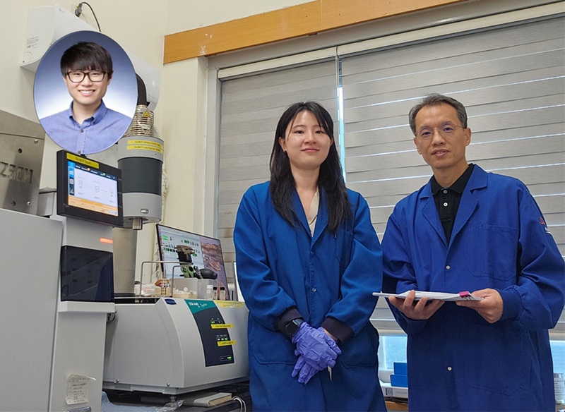 KAIST Uses AI to Discover Optimal New Material for Removing Radioactive Iodine Contamination
<(From the Right) Professor Ho Jin Ryu, Department of Nuclear and Quantum Engineering, Dr. Sujeong Lee, a graduate of the KAIST Department of Materials Science and Engineering, and Dr. Juhwan Noh of KRICT’s Digital Chemistry Research Center>
Managing radioactive waste is one of the core challenges in the use of nuclear energy. In particular, radioactive iodine poses serious environmental and health risks due to its long half-life (15.7 million years in the case of I-129), high mobility, and toxicity to living organisms. A Korean research team has successfully used artificial intelligence to discover a new material that can remove iodine for nuclear environmental remediation. The team plans to push forward with commercialization through various industry-academia collaborations, from iodine-adsorbing powders to contaminated water treatment filters.
KAIST (President Kwang Hyung Lee) announced on the 2of July that Professor Ho Jin Ryu's research team from the Department of Nuclear and Quantum Engineering, in collaboration with Dr. Juhwan Noh of the Digital Chemistry Research Center at the Korea Research Institute of Chemical Technology (KRICT, President Young Kook Lee), which operates under the National Research Council of Science & Technology (NST, Chairman Youngsik Kim), developed a technique using AI to discover new materials that effectively remove radioactive iodine contaminants.
Recent studies show that radioactive iodine primarily exists in aqueous environments in the form of iodate (IO₃⁻). However, existing silver-based adsorbents have weak chemical adsorption strength for iodate, making them inefficient. Therefore, it is imperative to develop new adsorbent materials that can effectively remove iodate.
Professor Ho Jin Ryu’s team used a machine learning-based experimental strategy to identify optimal iodate adsorbents among compounds called Layered Double Hydroxides (LDHs), which contain various metal elements.
The multi-metal LDH developed in this study – Cu₃(CrFeAl), based on copper, chromium, iron, and aluminum—showed exceptional adsorption performance, removing over 90% of iodate. This achievement was made possible by efficiently exploring a vast compositional space using AI-driven active learning, which would be difficult to search through conventional trial-and-error experiments.
<Picture2. Concept of Developed AI-Based Technology for Exploring New Materials for Radioactive Contamination Removal>
The research team focused on the fact that LDHs, like high-entropy materials, can incorporate a wide range of metal compositions and possess structures favorable for anion adsorption. However, due to the overwhelming number of possible metal combinations in multi-metal LDHs, identifying the optimal composition through traditional experimental methods has been nearly impossible.
To overcome this, the team employed AI (machine learning). Starting with experimental data from 24 binary and 96 ternary LDH compositions, they expanded their search to include quaternary and quinary candidates. As a result, they were able to discover the optimal material for iodate removal by testing only 16% of the total candidate materials.
Professor Ho Jin Ryu stated, “This study shows the potential of using artificial intelligence to efficiently identify radioactive decontamination materials from a vast pool of new material candidates, which is expected to accelerate research for developing new materials for nuclear environmental cleanup.”
The research team has filed a domestic patent application for the developed powder technology and is currently proceeding with an international patent application. They plan to enhance the material’s performance under various conditions and pursue commercialization through industry-academia cooperation in the development of filters for treating contaminated water.
Dr. Sujeong Lee, a graduate of the KAIST Department of Materials Science and Engineering, and Dr. Juhwan Noh of KRICT’s Digital Chemistry Research Center, participated as the co-first authors of the study. The results were published online on May 26 in the internationally renowned environmental publication Journal of Hazardous Materials.
※ Paper title: Discovery of multi-metal-layered double hydroxides for decontamination of iodate by machine learning-assisted experiments ※ DOI: https://doi.org/10.1016/j.jhazmat.2025.138735
This research was supported by the Nuclear Energy Research Infrastructure Program and the Nano-Materials Technology Development Program funded by the Ministry of Science and ICT and the National Research Foundation of Korea.
2025.07.03 View 1353
KAIST Uses AI to Discover Optimal New Material for Removing Radioactive Iodine Contamination
<(From the Right) Professor Ho Jin Ryu, Department of Nuclear and Quantum Engineering, Dr. Sujeong Lee, a graduate of the KAIST Department of Materials Science and Engineering, and Dr. Juhwan Noh of KRICT’s Digital Chemistry Research Center>
Managing radioactive waste is one of the core challenges in the use of nuclear energy. In particular, radioactive iodine poses serious environmental and health risks due to its long half-life (15.7 million years in the case of I-129), high mobility, and toxicity to living organisms. A Korean research team has successfully used artificial intelligence to discover a new material that can remove iodine for nuclear environmental remediation. The team plans to push forward with commercialization through various industry-academia collaborations, from iodine-adsorbing powders to contaminated water treatment filters.
KAIST (President Kwang Hyung Lee) announced on the 2of July that Professor Ho Jin Ryu's research team from the Department of Nuclear and Quantum Engineering, in collaboration with Dr. Juhwan Noh of the Digital Chemistry Research Center at the Korea Research Institute of Chemical Technology (KRICT, President Young Kook Lee), which operates under the National Research Council of Science & Technology (NST, Chairman Youngsik Kim), developed a technique using AI to discover new materials that effectively remove radioactive iodine contaminants.
Recent studies show that radioactive iodine primarily exists in aqueous environments in the form of iodate (IO₃⁻). However, existing silver-based adsorbents have weak chemical adsorption strength for iodate, making them inefficient. Therefore, it is imperative to develop new adsorbent materials that can effectively remove iodate.
Professor Ho Jin Ryu’s team used a machine learning-based experimental strategy to identify optimal iodate adsorbents among compounds called Layered Double Hydroxides (LDHs), which contain various metal elements.
The multi-metal LDH developed in this study – Cu₃(CrFeAl), based on copper, chromium, iron, and aluminum—showed exceptional adsorption performance, removing over 90% of iodate. This achievement was made possible by efficiently exploring a vast compositional space using AI-driven active learning, which would be difficult to search through conventional trial-and-error experiments.
<Picture2. Concept of Developed AI-Based Technology for Exploring New Materials for Radioactive Contamination Removal>
The research team focused on the fact that LDHs, like high-entropy materials, can incorporate a wide range of metal compositions and possess structures favorable for anion adsorption. However, due to the overwhelming number of possible metal combinations in multi-metal LDHs, identifying the optimal composition through traditional experimental methods has been nearly impossible.
To overcome this, the team employed AI (machine learning). Starting with experimental data from 24 binary and 96 ternary LDH compositions, they expanded their search to include quaternary and quinary candidates. As a result, they were able to discover the optimal material for iodate removal by testing only 16% of the total candidate materials.
Professor Ho Jin Ryu stated, “This study shows the potential of using artificial intelligence to efficiently identify radioactive decontamination materials from a vast pool of new material candidates, which is expected to accelerate research for developing new materials for nuclear environmental cleanup.”
The research team has filed a domestic patent application for the developed powder technology and is currently proceeding with an international patent application. They plan to enhance the material’s performance under various conditions and pursue commercialization through industry-academia cooperation in the development of filters for treating contaminated water.
Dr. Sujeong Lee, a graduate of the KAIST Department of Materials Science and Engineering, and Dr. Juhwan Noh of KRICT’s Digital Chemistry Research Center, participated as the co-first authors of the study. The results were published online on May 26 in the internationally renowned environmental publication Journal of Hazardous Materials.
※ Paper title: Discovery of multi-metal-layered double hydroxides for decontamination of iodate by machine learning-assisted experiments ※ DOI: https://doi.org/10.1016/j.jhazmat.2025.138735
This research was supported by the Nuclear Energy Research Infrastructure Program and the Nano-Materials Technology Development Program funded by the Ministry of Science and ICT and the National Research Foundation of Korea.
2025.07.03 View 1353