electronic
-
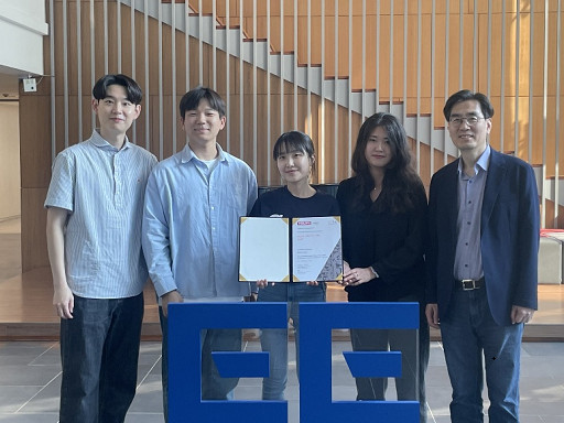
 Approaches to Human-Robot Interaction Using Biosignals
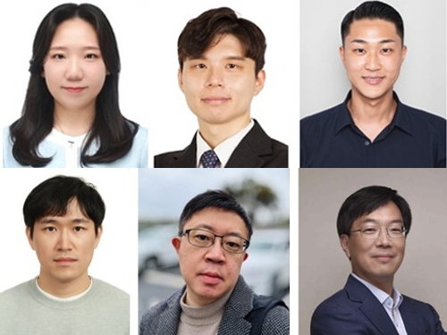
<(From left) Dr. Hwa-young Jeong, Professor Kyung-seo Park, Dr. Yoon-tae Jeong, Dr. Ji-hoon Seo, Professor Min-kyu Je, Professor Jung Kim >
A joint research team led by Professor Jung Kim of KAIST Department of Mechanical Engineering and Professor Min-kyu Je of the Department of Electrical and Electronic Engineering recently published a review paper on the latest trends and advancements in intuitive Human-Robot Interaction (HRI) using bio-potential and bio-impedance in the internationally renowned academic journal 'Nature Reviews Electrical Engineering'.
This review paper is the result of a collaborative effort by Dr. Kyung-seo Park (DGIST, co-first author), Dr. Hwa-young Jeong (EPFL, co-first author), Dr. Yoon-tae Jeong (IMEC), and Dr. Ji-hoon Seo (UCSD), all doctoral graduates from the two laboratories. Nature Reviews Electrical Engineering is a review specialized journal in the field of electrical, electronic, and artificial intelligence technology, newly launched by Nature Publishing Group last year. It is known to invite world-renowned scholars in the field through strict selection criteria. Professor Jung Kim's research team's paper, titled "Using bio-potential and bio-impedance for intuitive human-robot interaction," was published on July 18, 2025. (DOI: https://doi.org/10.1038/s44287-025-00191-5)
This review paper explains how biosignals can be used to quickly and accurately detect movement intentions and introduces advancements in movement prediction technology based on neural signals and muscle activity. It also focuses on the crucial role of integrated circuits (ICs) in maximizing low-noise performance and energy efficiency in biosignal sensing, covering thelatest development trends in low-noise, low-power designs for accurately measuring bio-potential and impedance signals.
The review emphasizes the importance of hybrid and multi-modal sensing approaches, presenting the possibility of building robust, intuitive, and scalable HRI systems. The research team stressed that collaboration between sensor and IC design fields is essential for the practical application of biosignal-based HRI systems and stated that interdisciplinary collaboration will play a significant role in the development of next-generation HRI technology. Dr. Hwa-young Jeong, a co-first author of the paper, presented the potential of bio-potential and impedance signals to make human-robot interaction more intuitive and efficient, predicting that it will make significant contributions to the development of HRI technologies such as rehabilitation robots and robotic prostheses using biosignals in the future. This research was supported by several research projects, including the Human Plus Project of the National Research Foundation of Korea.
2025.07.24 View 529
Approaches to Human-Robot Interaction Using Biosignals
<(From left) Dr. Hwa-young Jeong, Professor Kyung-seo Park, Dr. Yoon-tae Jeong, Dr. Ji-hoon Seo, Professor Min-kyu Je, Professor Jung Kim >
A joint research team led by Professor Jung Kim of KAIST Department of Mechanical Engineering and Professor Min-kyu Je of the Department of Electrical and Electronic Engineering recently published a review paper on the latest trends and advancements in intuitive Human-Robot Interaction (HRI) using bio-potential and bio-impedance in the internationally renowned academic journal 'Nature Reviews Electrical Engineering'.
This review paper is the result of a collaborative effort by Dr. Kyung-seo Park (DGIST, co-first author), Dr. Hwa-young Jeong (EPFL, co-first author), Dr. Yoon-tae Jeong (IMEC), and Dr. Ji-hoon Seo (UCSD), all doctoral graduates from the two laboratories. Nature Reviews Electrical Engineering is a review specialized journal in the field of electrical, electronic, and artificial intelligence technology, newly launched by Nature Publishing Group last year. It is known to invite world-renowned scholars in the field through strict selection criteria. Professor Jung Kim's research team's paper, titled "Using bio-potential and bio-impedance for intuitive human-robot interaction," was published on July 18, 2025. (DOI: https://doi.org/10.1038/s44287-025-00191-5)
This review paper explains how biosignals can be used to quickly and accurately detect movement intentions and introduces advancements in movement prediction technology based on neural signals and muscle activity. It also focuses on the crucial role of integrated circuits (ICs) in maximizing low-noise performance and energy efficiency in biosignal sensing, covering thelatest development trends in low-noise, low-power designs for accurately measuring bio-potential and impedance signals.
The review emphasizes the importance of hybrid and multi-modal sensing approaches, presenting the possibility of building robust, intuitive, and scalable HRI systems. The research team stressed that collaboration between sensor and IC design fields is essential for the practical application of biosignal-based HRI systems and stated that interdisciplinary collaboration will play a significant role in the development of next-generation HRI technology. Dr. Hwa-young Jeong, a co-first author of the paper, presented the potential of bio-potential and impedance signals to make human-robot interaction more intuitive and efficient, predicting that it will make significant contributions to the development of HRI technologies such as rehabilitation robots and robotic prostheses using biosignals in the future. This research was supported by several research projects, including the Human Plus Project of the National Research Foundation of Korea.
2025.07.24 View 529 -
 Professor Jung-woo' Choi ‘s Team Comes in First at the World's Top Acoustic AI Challenge
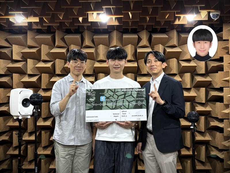
<Photo1. (From left) Ph.D candidate Yong-hoo Kwon, M.S candidate Do-hwan Kim, Professor Jung-woo Choi, Dr. Dong-heon Lee>
'Acoustic separation and classification technology' is a next-generation artificial intelligence (AI) core technology that enables the early detection of abnormal sounds in areas such as drones, fault detection of factory pipelines, and border surveillance systems, or allows for the separation and editing of spatial audio by sound source when producing AR/VR content.
On the 11th of July, a research team led by Professor Jung-woo Choi of KAIST's Department of Electrical and Electronic Engineering won first place in the 'Spatial Semantic Segmentation of Sound Scenes' task of the 'DCASE2025 Challenge,' the world's most prestigious acoustic detection and analysis competition.
This year’s challenge featured 86 teams competing across six tasks. In this competition, the KAIST research team achieved the best performance in their first-ever participation to Task 4. Professor Jung-woo Choi’s research team consisted of Dr. Dong-heon, Lee, Ph.D. candidate Young-hoo Kwon, and M.S. candidate Do-hwan Kim.
Task 4 titled 'Spatial Semantic Segmentation of Sound Scenes' is a highly demanding task requiring the analysis of spatial information in multi-channel audio signals with overlapping sound sources. The goal was to separate individual sounds and classify them into 18 predefined categories. The research team plans to present their technology at the DCASE workshop in Barcelona this October.
<Figure 1. Example of an acoustic scene with multiple mixed sounds>
Early this year, Dr. Dong-heon Lee developed a state-of-the-art sound source separation AI that combines Transformer and Mamba architectures. During the competition, centered around researcher Young-hoo Kwon, they completed a ‘chain-of-inference architecture' AI model that performs sound source separation and classification again, using the waveforms and types of the initially separated sound sources as clues. This AI model is inspired by human’s auditory scene analysis mechanism that isolates individual sounds by focusing on incomplete clues such as sound type, rhythm, or direction, when listening to complex sounds.
Through this, the team was the only participant to achieve double-digit performance (11 dB) in 'Class-Aware Signal-to-Distortion Ratio Improvement (CA-SDRi)*,' which is the measure for ranking how well the AI separated and classified sounds, proving their technical excellence.
Class-Aware Signal-to-Distortion Ratio Improvement (CA-SDRi): Measures how much clearer (less distorted) the desired sound is separated and classified compared to the original audio, in dB (decibels). A higher number indicates more accurate and cleaner sound separation.
Prof. Jung-woo Choi remarked, "The research team has showcased world-leading acoustic separation AI models for the past three years, and I am delighted that these results have been officially recognized." He added, "I am proud of every member of the research team for winning first place through focused research, despite the significant increase in difficulty and having only a few weeks for development."
<Figure 2. Time-frequency patterns of sound sources separated from a mixed source>
The IEEE DCASE Challenge 2025 was held online, with submissions accepted from April 1 to June 15 and results announced on June 30. Since its launch in 2013, the DCASE Challenge has served as a premier global platform of IEEE Signal Processing Society for showcasing cutting-edge AI models in acoustic signal processing.
This research was supported by the Mid-Career Researcher Support Project and STEAM Research Project of the National Research Foundation of Korea, funded by the Ministry of Education, Science and Technology, as well as support from the Future Defense Research Center, funded by the Defense Acquisition Program Administration and the Agency for Defense Development.
2025.07.13 View 480
Professor Jung-woo' Choi ‘s Team Comes in First at the World's Top Acoustic AI Challenge
<Photo1. (From left) Ph.D candidate Yong-hoo Kwon, M.S candidate Do-hwan Kim, Professor Jung-woo Choi, Dr. Dong-heon Lee>
'Acoustic separation and classification technology' is a next-generation artificial intelligence (AI) core technology that enables the early detection of abnormal sounds in areas such as drones, fault detection of factory pipelines, and border surveillance systems, or allows for the separation and editing of spatial audio by sound source when producing AR/VR content.
On the 11th of July, a research team led by Professor Jung-woo Choi of KAIST's Department of Electrical and Electronic Engineering won first place in the 'Spatial Semantic Segmentation of Sound Scenes' task of the 'DCASE2025 Challenge,' the world's most prestigious acoustic detection and analysis competition.
This year’s challenge featured 86 teams competing across six tasks. In this competition, the KAIST research team achieved the best performance in their first-ever participation to Task 4. Professor Jung-woo Choi’s research team consisted of Dr. Dong-heon, Lee, Ph.D. candidate Young-hoo Kwon, and M.S. candidate Do-hwan Kim.
Task 4 titled 'Spatial Semantic Segmentation of Sound Scenes' is a highly demanding task requiring the analysis of spatial information in multi-channel audio signals with overlapping sound sources. The goal was to separate individual sounds and classify them into 18 predefined categories. The research team plans to present their technology at the DCASE workshop in Barcelona this October.
<Figure 1. Example of an acoustic scene with multiple mixed sounds>
Early this year, Dr. Dong-heon Lee developed a state-of-the-art sound source separation AI that combines Transformer and Mamba architectures. During the competition, centered around researcher Young-hoo Kwon, they completed a ‘chain-of-inference architecture' AI model that performs sound source separation and classification again, using the waveforms and types of the initially separated sound sources as clues. This AI model is inspired by human’s auditory scene analysis mechanism that isolates individual sounds by focusing on incomplete clues such as sound type, rhythm, or direction, when listening to complex sounds.
Through this, the team was the only participant to achieve double-digit performance (11 dB) in 'Class-Aware Signal-to-Distortion Ratio Improvement (CA-SDRi)*,' which is the measure for ranking how well the AI separated and classified sounds, proving their technical excellence.
Class-Aware Signal-to-Distortion Ratio Improvement (CA-SDRi): Measures how much clearer (less distorted) the desired sound is separated and classified compared to the original audio, in dB (decibels). A higher number indicates more accurate and cleaner sound separation.
Prof. Jung-woo Choi remarked, "The research team has showcased world-leading acoustic separation AI models for the past three years, and I am delighted that these results have been officially recognized." He added, "I am proud of every member of the research team for winning first place through focused research, despite the significant increase in difficulty and having only a few weeks for development."
<Figure 2. Time-frequency patterns of sound sources separated from a mixed source>
The IEEE DCASE Challenge 2025 was held online, with submissions accepted from April 1 to June 15 and results announced on June 30. Since its launch in 2013, the DCASE Challenge has served as a premier global platform of IEEE Signal Processing Society for showcasing cutting-edge AI models in acoustic signal processing.
This research was supported by the Mid-Career Researcher Support Project and STEAM Research Project of the National Research Foundation of Korea, funded by the Ministry of Education, Science and Technology, as well as support from the Future Defense Research Center, funded by the Defense Acquisition Program Administration and the Agency for Defense Development.
2025.07.13 View 480 -
 Military Combatants Usher in an Era of Personalized Training with New Materials
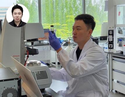
< Photo 1. (From left) Professor Steve Park of Materials Science and Engineering, Kyusoon Pak, Ph.D. Candidate (Army Major) >
Traditional military training often relies on standardized methods, which has limited the provision of optimized training tailored to individual combatants' characteristics or specific combat situations. To address this, our research team developed an e-textile platform, securing core technology that can reflect the unique traits of individual combatants and various combat scenarios. This technology has proven robust enough for battlefield use and is economical enough for widespread distribution to a large number of troops.
On June 25th, Professor Steve Park's research team at KAIST's Department of Materials Science and Engineering announced the development of a flexible, wearable electronic textile (E-textile) platform using an innovative technology that 'draws' electronic circuits directly onto fabric.
The wearable e-textile platform developed by the research team combines 3D printing technology with new materials engineering design to directly print flexible and highly durable sensors and electrodes onto textile substrates. This enables the collection of precise movement and human body data from individual combatants, which can then be used to propose customized training models.
Existing e-textile fabrication methods were often complex or limited in their ability to provide personalized customization. To overcome these challenges, the research team adopted an additive manufacturing technology called 'Direct Ink Writing (DIW)' 3D printing.
< Figure 1. Schematic diagram of e-textile manufactured with Direct Ink Writing (DIW) printing technology on various textiles, including combat uniforms >
This technology involves directly dispensing and printing special ink, which functions as sensors and electrodes, onto textile substrates in desired patterns. This allows for flexible implementation of various designs without the complex process of mask fabrication. This is expected to be an effective technology that can be easily supplied to hundreds of thousands of military personnel.
The core of this technology lies in the development of high-performance functional inks based on advanced materials engineering design. The research team combined styrene-butadiene-styrene (SBS) polymer, which provides flexibility, with multi-walled carbon nanotubes (MWCNT) for electrical conductivity. They developed a tensile/bending sensor ink that can stretch up to 102% and maintain stable performance even after 10,000 repetitive tests. This means that accurate data can be consistently obtained even during the strenuous movements of combatants.
< Figure 2. Measurement of human movement and breathing patterns using e-textile >
Furthermore, new material technology was applied to implement 'interconnect electrodes' that electrically connect the upper and lower layers of the fabric. The team developed an electrode ink combining silver (Ag) flakes with rigid polystyrene (PS) polymer, precisely controlling the impregnation level (how much the ink penetrates the fabric) to effectively connect both sides or multiple layers of the fabric. This secures the technology for producing multi-layered wearable electronic systems integrating sensors and electrodes.
< Figure 3. Experimental results of recognizing unknown objects after machine learning six objects using a smart glove >
The research team proved the platform's performance through actual human movement monitoring experiments. They printed the developed e-textile on major joint areas of clothing (shoulders, elbows, knees) and measured movements and posture changes during various exercises such as running, jumping jacks, and push-ups in real-time.
Additionally, they demonstrated the potential for applications such as monitoring breathing patterns using a smart mask and recognizing objects through machine learning and perceiving complex tactile information by printing multiple sensors and electrodes on gloves. These results show that the developed e-textile platform is effective in precisely understanding the movement dynamics of combatants.
This research is an important example demonstrating how cutting-edge new material technology can contribute to the advancement of the defense sector. Major Kyusoon Pak of the Army, who participated in this research, considered required objectives such as military applicability and economic feasibility for practical distribution from the research design stage.
< Figure 4. Experimental results showing that a multi-layered e-textile glove connected with interconnect electrodes can measure tensile/bending signals and pressure signals at a single point >
Major Pak stated, "Our military is currently facing both a crisis and an opportunity due to the decrease in military personnel resources caused by the demographic cliff and the advancement of science and technology. Also, respect for life in the battlefield is emerging as a significant issue. This research aims to secure original technology that can provide customized training according to military branch/duty and type of combat, thereby enhancing the combat power and ensuring the survivability of our soldiers."
He added, "I hope this research will be evaluated as a case that achieved both scientific contribution and military applicability."
This research, where Kyusoon Pak, Ph.D. Candidate (Army Major) from KAIST's Department of Materials Science and Engineering, participated as the first author and Professor Steve Park supervised, was published on May 27, 2025, in `npj Flexible Electronics (top 1.8% in JCR field)', an international academic journal in the electrical, electronic, and materials engineering fields.
* Paper Title: Fabrication of Multifunctional Wearable Interconnect E-textile Platform Using Direct Ink Writing (DIW) 3D Printing
* DOI: https://doi.org/10.1038/s41528-025-00414-7
This research was supported by the Ministry of Trade, Industry and Energy and the National Research Foundation of Korea.
2025.06.25 View 2098
Military Combatants Usher in an Era of Personalized Training with New Materials
< Photo 1. (From left) Professor Steve Park of Materials Science and Engineering, Kyusoon Pak, Ph.D. Candidate (Army Major) >
Traditional military training often relies on standardized methods, which has limited the provision of optimized training tailored to individual combatants' characteristics or specific combat situations. To address this, our research team developed an e-textile platform, securing core technology that can reflect the unique traits of individual combatants and various combat scenarios. This technology has proven robust enough for battlefield use and is economical enough for widespread distribution to a large number of troops.
On June 25th, Professor Steve Park's research team at KAIST's Department of Materials Science and Engineering announced the development of a flexible, wearable electronic textile (E-textile) platform using an innovative technology that 'draws' electronic circuits directly onto fabric.
The wearable e-textile platform developed by the research team combines 3D printing technology with new materials engineering design to directly print flexible and highly durable sensors and electrodes onto textile substrates. This enables the collection of precise movement and human body data from individual combatants, which can then be used to propose customized training models.
Existing e-textile fabrication methods were often complex or limited in their ability to provide personalized customization. To overcome these challenges, the research team adopted an additive manufacturing technology called 'Direct Ink Writing (DIW)' 3D printing.
< Figure 1. Schematic diagram of e-textile manufactured with Direct Ink Writing (DIW) printing technology on various textiles, including combat uniforms >
This technology involves directly dispensing and printing special ink, which functions as sensors and electrodes, onto textile substrates in desired patterns. This allows for flexible implementation of various designs without the complex process of mask fabrication. This is expected to be an effective technology that can be easily supplied to hundreds of thousands of military personnel.
The core of this technology lies in the development of high-performance functional inks based on advanced materials engineering design. The research team combined styrene-butadiene-styrene (SBS) polymer, which provides flexibility, with multi-walled carbon nanotubes (MWCNT) for electrical conductivity. They developed a tensile/bending sensor ink that can stretch up to 102% and maintain stable performance even after 10,000 repetitive tests. This means that accurate data can be consistently obtained even during the strenuous movements of combatants.
< Figure 2. Measurement of human movement and breathing patterns using e-textile >
Furthermore, new material technology was applied to implement 'interconnect electrodes' that electrically connect the upper and lower layers of the fabric. The team developed an electrode ink combining silver (Ag) flakes with rigid polystyrene (PS) polymer, precisely controlling the impregnation level (how much the ink penetrates the fabric) to effectively connect both sides or multiple layers of the fabric. This secures the technology for producing multi-layered wearable electronic systems integrating sensors and electrodes.
< Figure 3. Experimental results of recognizing unknown objects after machine learning six objects using a smart glove >
The research team proved the platform's performance through actual human movement monitoring experiments. They printed the developed e-textile on major joint areas of clothing (shoulders, elbows, knees) and measured movements and posture changes during various exercises such as running, jumping jacks, and push-ups in real-time.
Additionally, they demonstrated the potential for applications such as monitoring breathing patterns using a smart mask and recognizing objects through machine learning and perceiving complex tactile information by printing multiple sensors and electrodes on gloves. These results show that the developed e-textile platform is effective in precisely understanding the movement dynamics of combatants.
This research is an important example demonstrating how cutting-edge new material technology can contribute to the advancement of the defense sector. Major Kyusoon Pak of the Army, who participated in this research, considered required objectives such as military applicability and economic feasibility for practical distribution from the research design stage.
< Figure 4. Experimental results showing that a multi-layered e-textile glove connected with interconnect electrodes can measure tensile/bending signals and pressure signals at a single point >
Major Pak stated, "Our military is currently facing both a crisis and an opportunity due to the decrease in military personnel resources caused by the demographic cliff and the advancement of science and technology. Also, respect for life in the battlefield is emerging as a significant issue. This research aims to secure original technology that can provide customized training according to military branch/duty and type of combat, thereby enhancing the combat power and ensuring the survivability of our soldiers."
He added, "I hope this research will be evaluated as a case that achieved both scientific contribution and military applicability."
This research, where Kyusoon Pak, Ph.D. Candidate (Army Major) from KAIST's Department of Materials Science and Engineering, participated as the first author and Professor Steve Park supervised, was published on May 27, 2025, in `npj Flexible Electronics (top 1.8% in JCR field)', an international academic journal in the electrical, electronic, and materials engineering fields.
* Paper Title: Fabrication of Multifunctional Wearable Interconnect E-textile Platform Using Direct Ink Writing (DIW) 3D Printing
* DOI: https://doi.org/10.1038/s41528-025-00414-7
This research was supported by the Ministry of Trade, Industry and Energy and the National Research Foundation of Korea.
2025.06.25 View 2098 -
 KAIST Research Team Develops Electronic Ink for Room-Temperature Printing of High-Resolution, Variable-Stiffness Electronics
A team of researchers from KAIST and Seoul National University has developed a groundbreaking electronic ink that enables room-temperature printing of variable-stiffness circuits capable of switching between rigid and soft modes. This advancement marks a significant leap toward next-generation wearable, implantable, and robotic devices.
< Photo 1. (From left) Professor Jae-Woong Jeong and PhD candidate Simok Lee of the School of Electrical Engineering, (in separate bubbles, from left) Professor Gun-Hee Lee of Pusan National University, Professor Seongjun Park of Seoul National University, Professor Steve Park of the Department of Materials Science and Engineering>
Variable-stiffness electronics are at the forefront of adaptive technology, offering the ability for a single device to transition between rigid and soft modes depending on its use case. Gallium, a metal known for its high rigidity contrast between solid and liquid states, is a promising candidate for such applications. However, its use has been hindered by challenges including high surface tension, low viscosity, and undesirable phase transitions during manufacturing.
On June 4th, a research team led by Professor Jae-Woong Jeong from the School of Electrical Engineering at KAIST, Professor Seongjun Park from the Digital Healthcare Major at Seoul National University, and Professor Steve Park from the Department of Materials Science and Engineering at KAIST introduced a novel liquid metal electronic ink. This ink allows for micro-scale circuit printing – thinner than a human hair – at room temperature, with the ability to reversibly switch between rigid and soft modes depending on temperature.
The new ink combines printable viscosity with excellent electrical conductivity, enabling the creation of complex, high-resolution multilayer circuits comparable to commercial printed circuit boards (PCBs). These circuits can dynamically change stiffness in response to temperature, presenting new opportunities for multifunctional electronics, medical technologies, and robotics.
Conventional electronics typically have fixed form factors – either rigid for durability or soft for wearability. Rigid devices like smartphones and laptops offer robust performance but are uncomfortable when worn, while soft electronics are more comfortable but lack precise handling. As demand grows for devices that can adapt their stiffness to context, variable-stiffness electronics are becoming increasingly important.
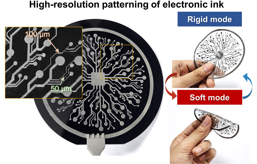
< Figure 1. Fabrication process of stable, high-viscosity electronic ink by dispersing micro-sized gallium particles in a polymer matrix (left). High-resolution large-area circuit printing process through pH-controlled chemical sintering (right). >
To address this challenge, the researchers focused on gallium, which melts just below body temperature. Solid gallium is quite stiff, while its liquid form is fluid and soft. Despite its potential, gallium’s use in electronic printing has been limited by its high surface tension and instability when melted.
To overcome these issues, the team developed a pH-controlled liquid metal ink printing process. By dispersing micro-sized gallium particles into a hydrophilic polyurethane matrix using a neutral solvent (dimethyl sulfoxide, or DMSO), they created a stable, high-viscosity ink suitable for precision printing. During post-print heating, the DMSO decomposes to form an acidic environment, which removes the oxide layer on the gallium particles. This triggers the particles to coalesce into electrically conductive networks with tunable mechanical properties.
The resulting printed circuits exhibit fine feature sizes (~50 μm), high conductivity (2.27 × 10⁶ S/m), and a stiffness modulation ratio of up to 1,465 – allowing the material to shift from plastic-like rigidity to rubber-like softness. Furthermore, the ink is compatible with conventional printing techniques such as screen printing and dip coating, supporting large-area and 3D device fabrication.
< Figure 2. Key features of the electronic ink. (i) High-resolution printing and multilayer integration capability. (ii) Batch fabrication capability through large-area screen printing. (iii) Complex three-dimensional structure printing capability through dip coating. (iv) Excellent electrical conductivity and stiffness control capability.>
The team demonstrated this technology by developing a multi-functional device that operates as a rigid portable electronic under normal conditions but transforms into a soft wearable healthcare device when attached to the body. They also created a neural probe that remains stiff during surgical insertion for accurate positioning but softens once inside brain tissue to reduce inflammation – highlighting its potential for biomedical implants.
< Figure 3. Variable stiffness wearable electronics with high-resolution circuits and multilayer structure comparable to commercial printed circuit boards (PCBs). Functions as a rigid portable electronic device at room temperature, then transforms into a wearable healthcare device by softening at body temperature upon skin contact.>
“The core achievement of this research lies in overcoming the longstanding challenges of liquid metal printing through our innovative technology,” said Professor Jeong. “By controlling the ink’s acidity, we were able to electrically and mechanically connect printed gallium particles, enabling the room-temperature fabrication of high-resolution, large-area circuits with tunable stiffness. This opens up new possibilities for future personal electronics, medical devices, and robotics.”
< Figure 4. Body-temperature softening neural probe implemented by coating electronic ink on an optical waveguide structure. (Left) Remains rigid during surgery for precise manipulation and brain insertion, then softens after implantation to minimize mechanical stress on the brain and greatly enhance biocompatibility. (Right) >
This research was published in Science Advances under the title, “Phase-Change Metal Ink with pH-Controlled Chemical Sintering for Versatile and Scalable Fabrication of Variable Stiffness Electronics.” The work was supported by the National Research Foundation of Korea, the Boston-Korea Project, and the BK21 FOUR Program.
2025.06.04 View 4072
KAIST Research Team Develops Electronic Ink for Room-Temperature Printing of High-Resolution, Variable-Stiffness Electronics
A team of researchers from KAIST and Seoul National University has developed a groundbreaking electronic ink that enables room-temperature printing of variable-stiffness circuits capable of switching between rigid and soft modes. This advancement marks a significant leap toward next-generation wearable, implantable, and robotic devices.
< Photo 1. (From left) Professor Jae-Woong Jeong and PhD candidate Simok Lee of the School of Electrical Engineering, (in separate bubbles, from left) Professor Gun-Hee Lee of Pusan National University, Professor Seongjun Park of Seoul National University, Professor Steve Park of the Department of Materials Science and Engineering>
Variable-stiffness electronics are at the forefront of adaptive technology, offering the ability for a single device to transition between rigid and soft modes depending on its use case. Gallium, a metal known for its high rigidity contrast between solid and liquid states, is a promising candidate for such applications. However, its use has been hindered by challenges including high surface tension, low viscosity, and undesirable phase transitions during manufacturing.
On June 4th, a research team led by Professor Jae-Woong Jeong from the School of Electrical Engineering at KAIST, Professor Seongjun Park from the Digital Healthcare Major at Seoul National University, and Professor Steve Park from the Department of Materials Science and Engineering at KAIST introduced a novel liquid metal electronic ink. This ink allows for micro-scale circuit printing – thinner than a human hair – at room temperature, with the ability to reversibly switch between rigid and soft modes depending on temperature.
The new ink combines printable viscosity with excellent electrical conductivity, enabling the creation of complex, high-resolution multilayer circuits comparable to commercial printed circuit boards (PCBs). These circuits can dynamically change stiffness in response to temperature, presenting new opportunities for multifunctional electronics, medical technologies, and robotics.
Conventional electronics typically have fixed form factors – either rigid for durability or soft for wearability. Rigid devices like smartphones and laptops offer robust performance but are uncomfortable when worn, while soft electronics are more comfortable but lack precise handling. As demand grows for devices that can adapt their stiffness to context, variable-stiffness electronics are becoming increasingly important.
< Figure 1. Fabrication process of stable, high-viscosity electronic ink by dispersing micro-sized gallium particles in a polymer matrix (left). High-resolution large-area circuit printing process through pH-controlled chemical sintering (right). >
To address this challenge, the researchers focused on gallium, which melts just below body temperature. Solid gallium is quite stiff, while its liquid form is fluid and soft. Despite its potential, gallium’s use in electronic printing has been limited by its high surface tension and instability when melted.
To overcome these issues, the team developed a pH-controlled liquid metal ink printing process. By dispersing micro-sized gallium particles into a hydrophilic polyurethane matrix using a neutral solvent (dimethyl sulfoxide, or DMSO), they created a stable, high-viscosity ink suitable for precision printing. During post-print heating, the DMSO decomposes to form an acidic environment, which removes the oxide layer on the gallium particles. This triggers the particles to coalesce into electrically conductive networks with tunable mechanical properties.
The resulting printed circuits exhibit fine feature sizes (~50 μm), high conductivity (2.27 × 10⁶ S/m), and a stiffness modulation ratio of up to 1,465 – allowing the material to shift from plastic-like rigidity to rubber-like softness. Furthermore, the ink is compatible with conventional printing techniques such as screen printing and dip coating, supporting large-area and 3D device fabrication.
< Figure 2. Key features of the electronic ink. (i) High-resolution printing and multilayer integration capability. (ii) Batch fabrication capability through large-area screen printing. (iii) Complex three-dimensional structure printing capability through dip coating. (iv) Excellent electrical conductivity and stiffness control capability.>
The team demonstrated this technology by developing a multi-functional device that operates as a rigid portable electronic under normal conditions but transforms into a soft wearable healthcare device when attached to the body. They also created a neural probe that remains stiff during surgical insertion for accurate positioning but softens once inside brain tissue to reduce inflammation – highlighting its potential for biomedical implants.
< Figure 3. Variable stiffness wearable electronics with high-resolution circuits and multilayer structure comparable to commercial printed circuit boards (PCBs). Functions as a rigid portable electronic device at room temperature, then transforms into a wearable healthcare device by softening at body temperature upon skin contact.>
“The core achievement of this research lies in overcoming the longstanding challenges of liquid metal printing through our innovative technology,” said Professor Jeong. “By controlling the ink’s acidity, we were able to electrically and mechanically connect printed gallium particles, enabling the room-temperature fabrication of high-resolution, large-area circuits with tunable stiffness. This opens up new possibilities for future personal electronics, medical devices, and robotics.”
< Figure 4. Body-temperature softening neural probe implemented by coating electronic ink on an optical waveguide structure. (Left) Remains rigid during surgery for precise manipulation and brain insertion, then softens after implantation to minimize mechanical stress on the brain and greatly enhance biocompatibility. (Right) >
This research was published in Science Advances under the title, “Phase-Change Metal Ink with pH-Controlled Chemical Sintering for Versatile and Scalable Fabrication of Variable Stiffness Electronics.” The work was supported by the National Research Foundation of Korea, the Boston-Korea Project, and the BK21 FOUR Program.
2025.06.04 View 4072 -
 Professor Hyun Myung's Team Wins First Place in a Challenge at ICRA by IEEE
< Photo 1. (From left) Daebeom Kim (Team Leader, Ph.D. student), Seungjae Lee (Ph.D. student), Seoyeon Jang (Ph.D. student), Jei Kong (Master's student), Professor Hyun Myung >
A team of the Urban Robotics Lab, led by Professor Hyun Myung from the KAIST School of Electrical Engineering, achieved a remarkable first-place overall victory in the Nothing Stands Still Challenge (NSS Challenge) 2025, held at the 2025 IEEE International Conference on Robotics and Automation (ICRA), the world's most prestigious robotics conference, from May 19 to 23 in Atlanta, USA.
The NSS Challenge was co-hosted by HILTI, a global construction company based in Liechtenstein, and Stanford University's Gradient Spaces Group. It is an expanded version of the HILTI SLAM (Simultaneous Localization and Mapping)* Challenge, which has been held since 2021, and is considered one of the most prominent challenges at 2025 IEEE ICRA.*SLAM: Refers to Simultaneous Localization and Mapping, a technology where robots, drones, autonomous vehicles, etc., determine their own position and simultaneously create a map of their surroundings.
< Photo 2. A scene from the oral presentation on the winning team's technology (Speakers: Seungjae Lee and Seoyeon Jang, Ph.D. candidates of KAIST School of Electrical Engineering) >
This challenge primarily evaluates how accurately and robustly LiDAR scan data, collected at various times, can be registered in situations with frequent structural changes, such as construction and industrial environments. In particular, it is regarded as a highly technical competition because it deals with multi-session localization and mapping (Multi-session SLAM) technology that responds to structural changes occurring over multiple timeframes, rather than just single-point registration accuracy.
The Urban Robotics Lab team secured first place overall, surpassing National Taiwan University (3rd place) and Northwestern Polytechnical University of China (2nd place) by a significant margin, with their unique localization and mapping technology that solves the problem of registering LiDAR data collected across multiple times and spaces. The winning team will be awarded a prize of $4,000.
< Figure 1. Example of Multiway-Registration for Registering Multiple Scans >
The Urban Robotics Lab team independently developed a multiway-registration framework that can robustly register multiple scans even without prior connection information. This framework consists of an algorithm for summarizing feature points within scans and finding correspondences (CubicFeat), an algorithm for performing global registration based on the found correspondences (Quatro), and an algorithm for refining results based on change detection (Chamelion). This combination of technologies ensures stable registration performance based on fixed structures, even in highly dynamic industrial environments.
< Figure 2. Example of Change Detection Using the Chamelion Algorithm>
LiDAR scan registration technology is a core component of SLAM (Simultaneous Localization And Mapping) in various autonomous systems such as autonomous vehicles, autonomous robots, autonomous walking systems, and autonomous flying vehicles.
Professor Hyun Myung of the School of Electrical Engineering stated, "This award-winning technology is evaluated as a case that simultaneously proves both academic value and industrial applicability by maximizing the performance of precisely estimating the relative positions between different scans even in complex environments. I am grateful to the students who challenged themselves and never gave up, even when many teams abandoned due to the high difficulty."
< Figure 3. Competition Result Board, Lower RMSE (Root Mean Squared Error) Indicates Higher Score (Unit: meters)>
The Urban Robotics Lab team first participated in the SLAM Challenge in 2022, winning second place among academic teams, and in 2023, they secured first place overall in the LiDAR category and first place among academic teams in the vision category.
2025.05.30 View 4839
Professor Hyun Myung's Team Wins First Place in a Challenge at ICRA by IEEE
< Photo 1. (From left) Daebeom Kim (Team Leader, Ph.D. student), Seungjae Lee (Ph.D. student), Seoyeon Jang (Ph.D. student), Jei Kong (Master's student), Professor Hyun Myung >
A team of the Urban Robotics Lab, led by Professor Hyun Myung from the KAIST School of Electrical Engineering, achieved a remarkable first-place overall victory in the Nothing Stands Still Challenge (NSS Challenge) 2025, held at the 2025 IEEE International Conference on Robotics and Automation (ICRA), the world's most prestigious robotics conference, from May 19 to 23 in Atlanta, USA.
The NSS Challenge was co-hosted by HILTI, a global construction company based in Liechtenstein, and Stanford University's Gradient Spaces Group. It is an expanded version of the HILTI SLAM (Simultaneous Localization and Mapping)* Challenge, which has been held since 2021, and is considered one of the most prominent challenges at 2025 IEEE ICRA.*SLAM: Refers to Simultaneous Localization and Mapping, a technology where robots, drones, autonomous vehicles, etc., determine their own position and simultaneously create a map of their surroundings.
< Photo 2. A scene from the oral presentation on the winning team's technology (Speakers: Seungjae Lee and Seoyeon Jang, Ph.D. candidates of KAIST School of Electrical Engineering) >
This challenge primarily evaluates how accurately and robustly LiDAR scan data, collected at various times, can be registered in situations with frequent structural changes, such as construction and industrial environments. In particular, it is regarded as a highly technical competition because it deals with multi-session localization and mapping (Multi-session SLAM) technology that responds to structural changes occurring over multiple timeframes, rather than just single-point registration accuracy.
The Urban Robotics Lab team secured first place overall, surpassing National Taiwan University (3rd place) and Northwestern Polytechnical University of China (2nd place) by a significant margin, with their unique localization and mapping technology that solves the problem of registering LiDAR data collected across multiple times and spaces. The winning team will be awarded a prize of $4,000.
< Figure 1. Example of Multiway-Registration for Registering Multiple Scans >
The Urban Robotics Lab team independently developed a multiway-registration framework that can robustly register multiple scans even without prior connection information. This framework consists of an algorithm for summarizing feature points within scans and finding correspondences (CubicFeat), an algorithm for performing global registration based on the found correspondences (Quatro), and an algorithm for refining results based on change detection (Chamelion). This combination of technologies ensures stable registration performance based on fixed structures, even in highly dynamic industrial environments.
< Figure 2. Example of Change Detection Using the Chamelion Algorithm>
LiDAR scan registration technology is a core component of SLAM (Simultaneous Localization And Mapping) in various autonomous systems such as autonomous vehicles, autonomous robots, autonomous walking systems, and autonomous flying vehicles.
Professor Hyun Myung of the School of Electrical Engineering stated, "This award-winning technology is evaluated as a case that simultaneously proves both academic value and industrial applicability by maximizing the performance of precisely estimating the relative positions between different scans even in complex environments. I am grateful to the students who challenged themselves and never gave up, even when many teams abandoned due to the high difficulty."
< Figure 3. Competition Result Board, Lower RMSE (Root Mean Squared Error) Indicates Higher Score (Unit: meters)>
The Urban Robotics Lab team first participated in the SLAM Challenge in 2022, winning second place among academic teams, and in 2023, they secured first place overall in the LiDAR category and first place among academic teams in the vision category.
2025.05.30 View 4839 -
 KAIST Demonstrates AI and sustainable technologies at CES 2024
On January 2, KAIST announced it will be participating in the Consumer Electronics Show (CES) 2024, held between January 9 and 12.
CES 2024 is one of the world’s largest tech conferences to take place in Las Vegas. Under the slogan “KAIST, the Global Value Creator” for its exhibition, KAIST has submitted technologies falling under one of following themes: “Expansion of Human Intelligence, Mobility, and Reality”, and “Pursuit of Human Security and Sustainable Development”.
24 startups and pre-startups whose technologies stand out in various fields including artificial intelligence (AI), mobility, virtual reality, healthcare and human security, and sustainable development, will welcome their visitors at an exclusive booth of 232 m2 prepared for KAIST at Eureka Park in Las Vegas.
12 businesses will participate in the first category, “Expansion of Human Intelligence, Mobility, and Reality”, including MicroPix, Panmnesia, DeepAuto, MGL, Reports, Narnia Labs, EL FACTORY, Korea Position Technology, AudAi, Planby Technologies, Movin, and Studio Lab.
In the “Pursuit of Human Security and Sustainable Development” category, 12 businesses including Aldaver, ADNC, Solve, Iris, Blue Device, Barreleye, TR, A2US, Greeners, Iron Boys, Shard Partners and Kingbot, will be introduced.
In particular, Aldaver is a startup that received the Korean Business Award 2023 as well as the presidential award at the Challenge K-Startup with its biomimetic material and printing technology. It has attracted 4.5 billion KRW of investment thus far.
Narnia Labs, with its AI design solution for manufacturing, won the grand prize for K-tech Startups 2022, and has so far attracted 3.5 billion KRW of investments.
Panmnesia is a startup that won the 2024 CES Innovation Award, recognized for their fab-less AI semiconductor technology. They attracted 16 billion KRW of investment through seed round alone.
Meanwhile, student startups will also be presented during the exhibition. Studio Lab received a CES 2024 Best of Innovation Award in the AI category. The team developed the software Seller Canvas, which automatically generates a page for product details when a user uploads an image of a product.
The central stage at the KAIST exhibition booth will be used to interview members of the participating startups between Jan 9 to 11, as well as a networking site for businesses and invited investors during KAIST NIGHT on the evening of 10th, between 5 and 7 PM.
Director Sung-Yool Choi of the KAIST Institute of Technology Value Creation said, “Through CES 2024, KAIST will overcome the limits of human intelligence, mobility, and space with the deep-tech based technologies developed by its startups, and will demonstrate its achievements for realizing its vision as a global value-creating university through the solutions for human security and sustainable development.”
2024.01.05 View 13064
KAIST Demonstrates AI and sustainable technologies at CES 2024
On January 2, KAIST announced it will be participating in the Consumer Electronics Show (CES) 2024, held between January 9 and 12.
CES 2024 is one of the world’s largest tech conferences to take place in Las Vegas. Under the slogan “KAIST, the Global Value Creator” for its exhibition, KAIST has submitted technologies falling under one of following themes: “Expansion of Human Intelligence, Mobility, and Reality”, and “Pursuit of Human Security and Sustainable Development”.
24 startups and pre-startups whose technologies stand out in various fields including artificial intelligence (AI), mobility, virtual reality, healthcare and human security, and sustainable development, will welcome their visitors at an exclusive booth of 232 m2 prepared for KAIST at Eureka Park in Las Vegas.
12 businesses will participate in the first category, “Expansion of Human Intelligence, Mobility, and Reality”, including MicroPix, Panmnesia, DeepAuto, MGL, Reports, Narnia Labs, EL FACTORY, Korea Position Technology, AudAi, Planby Technologies, Movin, and Studio Lab.
In the “Pursuit of Human Security and Sustainable Development” category, 12 businesses including Aldaver, ADNC, Solve, Iris, Blue Device, Barreleye, TR, A2US, Greeners, Iron Boys, Shard Partners and Kingbot, will be introduced.
In particular, Aldaver is a startup that received the Korean Business Award 2023 as well as the presidential award at the Challenge K-Startup with its biomimetic material and printing technology. It has attracted 4.5 billion KRW of investment thus far.
Narnia Labs, with its AI design solution for manufacturing, won the grand prize for K-tech Startups 2022, and has so far attracted 3.5 billion KRW of investments.
Panmnesia is a startup that won the 2024 CES Innovation Award, recognized for their fab-less AI semiconductor technology. They attracted 16 billion KRW of investment through seed round alone.
Meanwhile, student startups will also be presented during the exhibition. Studio Lab received a CES 2024 Best of Innovation Award in the AI category. The team developed the software Seller Canvas, which automatically generates a page for product details when a user uploads an image of a product.
The central stage at the KAIST exhibition booth will be used to interview members of the participating startups between Jan 9 to 11, as well as a networking site for businesses and invited investors during KAIST NIGHT on the evening of 10th, between 5 and 7 PM.
Director Sung-Yool Choi of the KAIST Institute of Technology Value Creation said, “Through CES 2024, KAIST will overcome the limits of human intelligence, mobility, and space with the deep-tech based technologies developed by its startups, and will demonstrate its achievements for realizing its vision as a global value-creating university through the solutions for human security and sustainable development.”
2024.01.05 View 13064 -
 KAIST to showcase a pack of KAIST Start-ups at CES 2023
- KAIST is to run an Exclusive Booth at the Venetian Expo (Hall G) in Eureka Park, at CES 2023, to be held in Las Vegas from Thursday, January 5th through Sunday, the 8th.
- Twelve businesses recently put together by KAIST faculty, alumni, and the start-ups given legal usage of KAIST technologies will be showcased.
- Out of the participating start-ups, the products by Fluiz and Hills Robotics were selected as the “CES Innovation Award 2023 Honoree”, scoring top in their respective categories.
On January 3, KAIST announced that there will be a KAIST booth at Consumer Electronics Show (CES) 2023, the most influential tech event in the world, to be held in Las Vegas from January 3 to 8.
At this exclusive corner, KAIST will introduce the technologies of KAIST start-ups over the exhibition period.
KAIST first started holding its exclusive booth in CES 2019 with five start-up businesses, following up at CES 2020 with 12 start-ups and at CES 2022 with 10 start-ups. At CES 2023, which would be KAIST’s fourth conference, KAIST will be accompanying 12 businesses including start-ups by the faculty members, alumni, and technology transfer companies that just began their businesses with technologies from their research findings that stands a head above others.
To maximize the publicity opportunity, KAIST will support each company’s marketing strategies through cooperation with the Korea International Trade Association (KITA), and provide an opportunity for the school and each startup to create global identity and exhibit the excellence of their technologies at the convention.
The following companies will be at the KAIST Booth in Eureka Park:
The twelve startups mentioned above aim to achieve global technology commecialization in their respective fields of expertise spanning from eXtended Reality (XR) and gaming, to AI and robotics, vehicle and transport, mobile platform, smart city, autonomous driving, healthcare, internet of thing (IoT), through joint research and development, technology transfer and investment attraction from world’s leading institutions and enterprises.
In particular, Fluiz and Hills Robotics won the CES Innovation Award as 2023 Honorees and is expected to attain greater achievements in the future.
A staff member from the KAIST Institute of Technology Value Creation said, “The KAIST Showcase for CES 2023 has prepared a new pitching space for each of the companies for their own IR efforts, and we hope that KAIST startups will actively and effectively market their products and technologies while they are at the convention. We hope it will help them utilize their time here to establish their name in presence here which will eventually serve as a good foothold for them and their predecessors to further global commercialization goals.”
2023.01.04 View 19755
KAIST to showcase a pack of KAIST Start-ups at CES 2023
- KAIST is to run an Exclusive Booth at the Venetian Expo (Hall G) in Eureka Park, at CES 2023, to be held in Las Vegas from Thursday, January 5th through Sunday, the 8th.
- Twelve businesses recently put together by KAIST faculty, alumni, and the start-ups given legal usage of KAIST technologies will be showcased.
- Out of the participating start-ups, the products by Fluiz and Hills Robotics were selected as the “CES Innovation Award 2023 Honoree”, scoring top in their respective categories.
On January 3, KAIST announced that there will be a KAIST booth at Consumer Electronics Show (CES) 2023, the most influential tech event in the world, to be held in Las Vegas from January 3 to 8.
At this exclusive corner, KAIST will introduce the technologies of KAIST start-ups over the exhibition period.
KAIST first started holding its exclusive booth in CES 2019 with five start-up businesses, following up at CES 2020 with 12 start-ups and at CES 2022 with 10 start-ups. At CES 2023, which would be KAIST’s fourth conference, KAIST will be accompanying 12 businesses including start-ups by the faculty members, alumni, and technology transfer companies that just began their businesses with technologies from their research findings that stands a head above others.
To maximize the publicity opportunity, KAIST will support each company’s marketing strategies through cooperation with the Korea International Trade Association (KITA), and provide an opportunity for the school and each startup to create global identity and exhibit the excellence of their technologies at the convention.
The following companies will be at the KAIST Booth in Eureka Park:
The twelve startups mentioned above aim to achieve global technology commecialization in their respective fields of expertise spanning from eXtended Reality (XR) and gaming, to AI and robotics, vehicle and transport, mobile platform, smart city, autonomous driving, healthcare, internet of thing (IoT), through joint research and development, technology transfer and investment attraction from world’s leading institutions and enterprises.
In particular, Fluiz and Hills Robotics won the CES Innovation Award as 2023 Honorees and is expected to attain greater achievements in the future.
A staff member from the KAIST Institute of Technology Value Creation said, “The KAIST Showcase for CES 2023 has prepared a new pitching space for each of the companies for their own IR efforts, and we hope that KAIST startups will actively and effectively market their products and technologies while they are at the convention. We hope it will help them utilize their time here to establish their name in presence here which will eventually serve as a good foothold for them and their predecessors to further global commercialization goals.”
2023.01.04 View 19755 -
 Atomically-Smooth Gold Crystals Help to Compress Light for Nanophotonic Applications
Highly compressed mid-infrared optical waves in a thin dielectric crystal on monocrystalline gold substrate investigated for the first time using a high-resolution scattering-type scanning near-field optical microscope.
KAIST researchers and their collaborators at home and abroad have successfully demonstrated a new platform for guiding the compressed light waves in very thin van der Waals crystals. Their method to guide the mid-infrared light with minimal loss will provide a breakthrough for the practical applications of ultra-thin dielectric crystals in next-generation optoelectronic devices based on strong light-matter interactions at the nanoscale.
Phonon-polaritons are collective oscillations of ions in polar dielectrics coupled to electromagnetic waves of light, whose electromagnetic field is much more compressed compared to the light wavelength. Recently, it was demonstrated that the phonon-polaritons in thin van der Waals crystals can be compressed even further when the material is placed on top of a highly conductive metal. In such a configuration, charges in the polaritonic crystal are “reflected” in the metal, and their coupling with light results in a new type of polariton waves called the image phonon-polaritons. Highly compressed image modes provide strong light-matter interactions, but are very sensitive to the substrate roughness, which hinders their practical application.
Challenged by these limitations, four research groups combined their efforts to develop a unique experimental platform using advanced fabrication and measurement methods. Their findings were published in Science Advances on July 13.
A KAIST research team led by Professor Min Seok Jang from the School of Electrical Engineering used a highly sensitive scanning near-field optical microscope (SNOM) to directly measure the optical fields of the hyperbolic image phonon-polaritons (HIP) propagating in a 63 nm-thick slab of hexagonal boron nitride (h-BN) on a monocrystalline gold substrate, showing the mid-infrared light waves in dielectric crystal compressed by a hundred times.
Professor Jang and a research professor in his group, Sergey Menabde, successfully obtained direct images of HIP waves propagating for many wavelengths, and detected a signal from the ultra-compressed high-order HIP in a regular h-BN crystals for the first time. They showed that the phonon-polaritons in van der Waals crystals can be significantly more compressed without sacrificing their lifetime.
This became possible due to the atomically-smooth surfaces of the home-grown gold crystals used as a substrate for the h-BN. Practically zero surface scattering and extremely small ohmic loss in gold at mid-infrared frequencies provide a low-loss environment for the HIP propagation. The HIP mode probed by the researchers was 2.4 times more compressed and yet exhibited a similar lifetime compared to the phonon-polaritons with a low-loss dielectric substrate, resulting in a twice higher figure of merit in terms of the normalized propagation length.
The ultra-smooth monocrystalline gold flakes used in the experiment were chemically grown by the team of Professor N. Asger Mortensen from the Center for Nano Optics at the University of Southern Denmark.
Mid-infrared spectrum is particularly important for sensing applications since many important organic molecules have absorption lines in the mid-infrared. However, a large number of molecules is required by the conventional detection methods for successful operation, whereas the ultra-compressed phonon-polariton fields can provide strong light-matter interactions at the microscopic level, thus significantly improving the detection limit down to a single molecule. The long lifetime of the HIP on monocrystalline gold will further improve the detection performance.
Furthermore, the study conducted by Professor Jang and the team demonstrated the striking similarity between the HIP and the image graphene plasmons. Both image modes possess significantly more confined electromagnetic field, yet their lifetime remains unaffected by the shorter polariton wavelength. This observation provides a broader perspective on image polaritons in general, and highlights their superiority in terms of the nanolight waveguiding compared to the conventional low-dimensional polaritons in van der Waals crystals on a dielectric substrate.
Professor Jang said, “Our research demonstrated the advantages of image polaritons, and especially the image phonon-polaritons. These optical modes can be used in the future optoelectronic devices where both the low-loss propagation and the strong light-matter interaction are necessary. I hope that our results will pave the way for the realization of more efficient nanophotonic devices such as metasurfaces, optical switches, sensors, and other applications operating at infrared frequencies.”
This research was funded by the Samsung Research Funding & Incubation Center of Samsung Electronics and the National Research Foundation of Korea (NRF). The Korea Institute of Science and Technology, Ministry of Education, Culture, Sports, Science and Technology of Japan, and The Villum Foundation, Denmark, also supported the work.
Figure. Nano-tip is used for the ultra-high-resolution imaging of the image phonon-polaritons in hBN launched by the gold crystal edge.
Publication:
Menabde, S. G., et al. (2022) Near-field probing of image phonon-polaritons in hexagonal boron nitride on gold crystals. Science Advances 8, Article ID: eabn0627. Available online at https://science.org/doi/10.1126/sciadv.abn0627.
Profile:
Min Seok Jang, MS, PhD
Associate Professor
jang.minseok@kaist.ac.kr
http://janglab.org/
Min Seok Jang Research Group
School of Electrical Engineering
http://kaist.ac.kr/en/
Korea Advanced Institute of Science and Technology (KAIST)
Daejeon, Republic of Korea
2022.07.13 View 17139
Atomically-Smooth Gold Crystals Help to Compress Light for Nanophotonic Applications
Highly compressed mid-infrared optical waves in a thin dielectric crystal on monocrystalline gold substrate investigated for the first time using a high-resolution scattering-type scanning near-field optical microscope.
KAIST researchers and their collaborators at home and abroad have successfully demonstrated a new platform for guiding the compressed light waves in very thin van der Waals crystals. Their method to guide the mid-infrared light with minimal loss will provide a breakthrough for the practical applications of ultra-thin dielectric crystals in next-generation optoelectronic devices based on strong light-matter interactions at the nanoscale.
Phonon-polaritons are collective oscillations of ions in polar dielectrics coupled to electromagnetic waves of light, whose electromagnetic field is much more compressed compared to the light wavelength. Recently, it was demonstrated that the phonon-polaritons in thin van der Waals crystals can be compressed even further when the material is placed on top of a highly conductive metal. In such a configuration, charges in the polaritonic crystal are “reflected” in the metal, and their coupling with light results in a new type of polariton waves called the image phonon-polaritons. Highly compressed image modes provide strong light-matter interactions, but are very sensitive to the substrate roughness, which hinders their practical application.
Challenged by these limitations, four research groups combined their efforts to develop a unique experimental platform using advanced fabrication and measurement methods. Their findings were published in Science Advances on July 13.
A KAIST research team led by Professor Min Seok Jang from the School of Electrical Engineering used a highly sensitive scanning near-field optical microscope (SNOM) to directly measure the optical fields of the hyperbolic image phonon-polaritons (HIP) propagating in a 63 nm-thick slab of hexagonal boron nitride (h-BN) on a monocrystalline gold substrate, showing the mid-infrared light waves in dielectric crystal compressed by a hundred times.
Professor Jang and a research professor in his group, Sergey Menabde, successfully obtained direct images of HIP waves propagating for many wavelengths, and detected a signal from the ultra-compressed high-order HIP in a regular h-BN crystals for the first time. They showed that the phonon-polaritons in van der Waals crystals can be significantly more compressed without sacrificing their lifetime.
This became possible due to the atomically-smooth surfaces of the home-grown gold crystals used as a substrate for the h-BN. Practically zero surface scattering and extremely small ohmic loss in gold at mid-infrared frequencies provide a low-loss environment for the HIP propagation. The HIP mode probed by the researchers was 2.4 times more compressed and yet exhibited a similar lifetime compared to the phonon-polaritons with a low-loss dielectric substrate, resulting in a twice higher figure of merit in terms of the normalized propagation length.
The ultra-smooth monocrystalline gold flakes used in the experiment were chemically grown by the team of Professor N. Asger Mortensen from the Center for Nano Optics at the University of Southern Denmark.
Mid-infrared spectrum is particularly important for sensing applications since many important organic molecules have absorption lines in the mid-infrared. However, a large number of molecules is required by the conventional detection methods for successful operation, whereas the ultra-compressed phonon-polariton fields can provide strong light-matter interactions at the microscopic level, thus significantly improving the detection limit down to a single molecule. The long lifetime of the HIP on monocrystalline gold will further improve the detection performance.
Furthermore, the study conducted by Professor Jang and the team demonstrated the striking similarity between the HIP and the image graphene plasmons. Both image modes possess significantly more confined electromagnetic field, yet their lifetime remains unaffected by the shorter polariton wavelength. This observation provides a broader perspective on image polaritons in general, and highlights their superiority in terms of the nanolight waveguiding compared to the conventional low-dimensional polaritons in van der Waals crystals on a dielectric substrate.
Professor Jang said, “Our research demonstrated the advantages of image polaritons, and especially the image phonon-polaritons. These optical modes can be used in the future optoelectronic devices where both the low-loss propagation and the strong light-matter interaction are necessary. I hope that our results will pave the way for the realization of more efficient nanophotonic devices such as metasurfaces, optical switches, sensors, and other applications operating at infrared frequencies.”
This research was funded by the Samsung Research Funding & Incubation Center of Samsung Electronics and the National Research Foundation of Korea (NRF). The Korea Institute of Science and Technology, Ministry of Education, Culture, Sports, Science and Technology of Japan, and The Villum Foundation, Denmark, also supported the work.
Figure. Nano-tip is used for the ultra-high-resolution imaging of the image phonon-polaritons in hBN launched by the gold crystal edge.
Publication:
Menabde, S. G., et al. (2022) Near-field probing of image phonon-polaritons in hexagonal boron nitride on gold crystals. Science Advances 8, Article ID: eabn0627. Available online at https://science.org/doi/10.1126/sciadv.abn0627.
Profile:
Min Seok Jang, MS, PhD
Associate Professor
jang.minseok@kaist.ac.kr
http://janglab.org/
Min Seok Jang Research Group
School of Electrical Engineering
http://kaist.ac.kr/en/
Korea Advanced Institute of Science and Technology (KAIST)
Daejeon, Republic of Korea
2022.07.13 View 17139 -
 KAA Recognizes 4 Distinguished Alumni of the Year
The KAIST Alumni Association (KAA) recognized four distinguished alumni of the year during a ceremony on February 25 in Seoul. The four Distinguished Alumni Awardees are Distinguished Professor Sukbok Chang from the KAIST Department of Chemistry, Hyunshil Ahn, head of the AI Economy Institute and an editorial writer at The Korea Economic Daily, CEO Hwan-ho Sung of PSTech, and President Hark Kyu Park of Samsung Electronics.
Distinguished Professor Sukbok Chang who received his MS from the Department of Chemistry in 1985 has been a pioneer in the novel field of ‘carbon-hydrogen bond activation reactions’. He has significantly contributed to raising Korea’s international reputation in natural sciences and received the Kyungam Academic Award in 2013, the 14th Korea Science Award in 2015, the 1st Science and Technology Prize of Korea Toray in 2018, and the Best Scientist/Engineer Award Korea in 2019. Furthermore, he was named as a Highly Cited Researcher who ranked in the top 1% of citations by field and publication year in the Web of Science citation index for seven consecutive years from 2015 to 2021, demonstrating his leadership as a global scholar.
Hyunshil Ahn, a graduate of the School of Business and Technology Management with an MS in 1985 and a PhD in 1987, was appointed as the first head of the AI Economy Institute when The Korea Economic Daily was the first Korean media outlet to establish an AI economy lab. He has contributed to creating new roles for the press and media in the 4th industrial revolution, and added to the popularization of AI technology through regulation reform and consulting on industrial policies.
PSTech CEO Hwan-ho Sung is a graduate of the School of Electrical Engineering where he received an MS in 1988 and a PhD in EMBA in 2008. He has run the electronics company PSTech for over 20 years and successfully localized the production of power equipment, which previously depended on foreign technology. His development of the world’s first power equipment that can be applied to new industries including semiconductors and displays was recognized through this award.
Samsung Electronics President Hark Kyu Park graduated from the School of Business and Technology Management with an MS in 1986. He not only enhanced Korea’s national competitiveness by expanding the semiconductor industry, but also established contract-based semiconductor departments at Korean universities including KAIST, Sungkyunkwan University, Yonsei University, and Postech, and semiconductor track courses at KAIST, Sogang University, Seoul National University, and Postech to nurture professional talents. He also led the national semiconductor coexistence system by leading private sector-government-academia collaborations to strengthen competence in semiconductors, and continues to make unconditional investments in strong small businesses.
KAA President Chilhee Chung said, “Thanks to our alumni contributing at the highest levels of our society, the name of our alma mater shines brighter. As role models for our younger alumni, I hope greater honours will follow our awardees in the future.”
2022.03.03 View 9689
KAA Recognizes 4 Distinguished Alumni of the Year
The KAIST Alumni Association (KAA) recognized four distinguished alumni of the year during a ceremony on February 25 in Seoul. The four Distinguished Alumni Awardees are Distinguished Professor Sukbok Chang from the KAIST Department of Chemistry, Hyunshil Ahn, head of the AI Economy Institute and an editorial writer at The Korea Economic Daily, CEO Hwan-ho Sung of PSTech, and President Hark Kyu Park of Samsung Electronics.
Distinguished Professor Sukbok Chang who received his MS from the Department of Chemistry in 1985 has been a pioneer in the novel field of ‘carbon-hydrogen bond activation reactions’. He has significantly contributed to raising Korea’s international reputation in natural sciences and received the Kyungam Academic Award in 2013, the 14th Korea Science Award in 2015, the 1st Science and Technology Prize of Korea Toray in 2018, and the Best Scientist/Engineer Award Korea in 2019. Furthermore, he was named as a Highly Cited Researcher who ranked in the top 1% of citations by field and publication year in the Web of Science citation index for seven consecutive years from 2015 to 2021, demonstrating his leadership as a global scholar.
Hyunshil Ahn, a graduate of the School of Business and Technology Management with an MS in 1985 and a PhD in 1987, was appointed as the first head of the AI Economy Institute when The Korea Economic Daily was the first Korean media outlet to establish an AI economy lab. He has contributed to creating new roles for the press and media in the 4th industrial revolution, and added to the popularization of AI technology through regulation reform and consulting on industrial policies.
PSTech CEO Hwan-ho Sung is a graduate of the School of Electrical Engineering where he received an MS in 1988 and a PhD in EMBA in 2008. He has run the electronics company PSTech for over 20 years and successfully localized the production of power equipment, which previously depended on foreign technology. His development of the world’s first power equipment that can be applied to new industries including semiconductors and displays was recognized through this award.
Samsung Electronics President Hark Kyu Park graduated from the School of Business and Technology Management with an MS in 1986. He not only enhanced Korea’s national competitiveness by expanding the semiconductor industry, but also established contract-based semiconductor departments at Korean universities including KAIST, Sungkyunkwan University, Yonsei University, and Postech, and semiconductor track courses at KAIST, Sogang University, Seoul National University, and Postech to nurture professional talents. He also led the national semiconductor coexistence system by leading private sector-government-academia collaborations to strengthen competence in semiconductors, and continues to make unconditional investments in strong small businesses.
KAA President Chilhee Chung said, “Thanks to our alumni contributing at the highest levels of our society, the name of our alma mater shines brighter. As role models for our younger alumni, I hope greater honours will follow our awardees in the future.”
2022.03.03 View 9689 -
 President Lee Presents Plans to Nurture Next-Generation Talents
President Lee stressed that nurturing medical scientists, semiconductor R&D personnel, startup entrepreneurs, and global innovators are key missions he will continue to pursue during a news conference
KAIST President Kwang Hyung Lee said that nurturing medical scientists, semiconductor R&D personnel, startup entrepreneurs, and global innovators are key missions he will continue to pursue during an online news conference marking the 1st anniversary of him becoming the president on February 15.
He said that nurturing physician-scientists is the most critical mission for KAIST to help the nation create a new growth engine. He said KAIST will help the nation drive the bio-industry and provide medical science resources for the nation’s health sector. To this end, he said that KAIST will open its Medical Science and Technology School by 2026.
“We plan to expand the current Graduate School of Medical Science and Engineering into a new Medical Science and Technology School that will focus entirely on a condensed MD-PhD course converging the fields of AI, bio, and physics,” he said.
The school aims to foster medical scientists whose research results will eventually be commercialized. He said that the university is now discussing revisions to related laws and regulations with the government and other universities.
To supply human resources to the semiconductor industry, President Lee said the university will add a campus in Pyongtaek City that will serve as an advanced convergence research hub in the field of next generation semiconductors in collaboration with Samsung Electronics and the city of Pyongtaek. The three-stage opening plan projected the final opening of the campus by 2036. During the first stage, which will be completed by 2026, it will construct the campus infrastructure in Pyongtaek city where Samsung Semiconductors runs two massive semiconductor complexes. By 2031, it plans to launch the open research platform including a future cities research center and future vehicles research center. The campus will open the global industrial collaboration cluster hub by 2036.
In the global arena, President Lee said he is working to open the New York campus with stakeholders in the United States. He announced the plan last December that was endorsed by New York-based entrepreneur Hee-Nam Bae, the chairman of Big Continent Inc. President Lee and Chairman Lee signed an MOU for the funding to open the campus in New York.
“We are discussing how to facilitate the plan and best accommodate the interests and potential of our students. Many ideas and plans are on the table and we think it will take longer than expected to finalize the plan,” explained President Lee.
However, he added that the basic idea is to offer art tech and health technology programs as well as an AI-based finance MBA at the New York campus, in addition to it serving as the startup accelerator of KAIST.
President Lee stressed the importance of technology commercialization when successfully launching KAIST Holdings last month to help spinoffs of KAIST labs accelerate their end results. He said that KAIST Holdings will build a virtuous supporting system to commercialize the technology startups coming from KAIST.
“We plan to list at least 10 KAIST startups on the KOSDAQ and two on the NASDAQ by 2031. KAIST Holdings also aims to nurture companies valued at a total of one billion KRW and earn 100 billion KRW in technology fees by 2031.
2022.02.17 View 14038
President Lee Presents Plans to Nurture Next-Generation Talents
President Lee stressed that nurturing medical scientists, semiconductor R&D personnel, startup entrepreneurs, and global innovators are key missions he will continue to pursue during a news conference
KAIST President Kwang Hyung Lee said that nurturing medical scientists, semiconductor R&D personnel, startup entrepreneurs, and global innovators are key missions he will continue to pursue during an online news conference marking the 1st anniversary of him becoming the president on February 15.
He said that nurturing physician-scientists is the most critical mission for KAIST to help the nation create a new growth engine. He said KAIST will help the nation drive the bio-industry and provide medical science resources for the nation’s health sector. To this end, he said that KAIST will open its Medical Science and Technology School by 2026.
“We plan to expand the current Graduate School of Medical Science and Engineering into a new Medical Science and Technology School that will focus entirely on a condensed MD-PhD course converging the fields of AI, bio, and physics,” he said.
The school aims to foster medical scientists whose research results will eventually be commercialized. He said that the university is now discussing revisions to related laws and regulations with the government and other universities.
To supply human resources to the semiconductor industry, President Lee said the university will add a campus in Pyongtaek City that will serve as an advanced convergence research hub in the field of next generation semiconductors in collaboration with Samsung Electronics and the city of Pyongtaek. The three-stage opening plan projected the final opening of the campus by 2036. During the first stage, which will be completed by 2026, it will construct the campus infrastructure in Pyongtaek city where Samsung Semiconductors runs two massive semiconductor complexes. By 2031, it plans to launch the open research platform including a future cities research center and future vehicles research center. The campus will open the global industrial collaboration cluster hub by 2036.
In the global arena, President Lee said he is working to open the New York campus with stakeholders in the United States. He announced the plan last December that was endorsed by New York-based entrepreneur Hee-Nam Bae, the chairman of Big Continent Inc. President Lee and Chairman Lee signed an MOU for the funding to open the campus in New York.
“We are discussing how to facilitate the plan and best accommodate the interests and potential of our students. Many ideas and plans are on the table and we think it will take longer than expected to finalize the plan,” explained President Lee.
However, he added that the basic idea is to offer art tech and health technology programs as well as an AI-based finance MBA at the New York campus, in addition to it serving as the startup accelerator of KAIST.
President Lee stressed the importance of technology commercialization when successfully launching KAIST Holdings last month to help spinoffs of KAIST labs accelerate their end results. He said that KAIST Holdings will build a virtuous supporting system to commercialize the technology startups coming from KAIST.
“We plan to list at least 10 KAIST startups on the KOSDAQ and two on the NASDAQ by 2031. KAIST Holdings also aims to nurture companies valued at a total of one billion KRW and earn 100 billion KRW in technology fees by 2031.
2022.02.17 View 14038 -
 Eco-Friendly Micro-Supercapacitors Using Fallen Leaves
Green micro-supercapacitors on a single leaf could easily be applied in wearable electronics, smart houses, and IoTs
A KAIST research team has developed graphene-inorganic-hybrid micro-supercapacitors made of fallen leaves using femtosecond laser direct writing. The rapid development of wearable electronics requires breakthrough innovations in flexible energy storage devices in which micro-supercapacitors have drawn a great deal of interest due to their high power density, long lifetimes, and short charging times. Recently, there has been an enormous increase in waste batteries owing to the growing demand and the shortened replacement cycle in consumer electronics. The safety and environmental issues involved in the collection, recycling, and processing of such waste batteries are creating a number of challenges.
Forests cover about 30 percent of the Earth’s surface and produce a huge amount of fallen leaves. This naturally occurring biomass comes in large quantities and is completely biodegradable, which makes it an attractive sustainable resource. Nevertheless, if the fallen leaves are left neglected instead of being used efficiently, they can contribute to fire hazards, air pollution, and global warming.
To solve both problems at once, a research team led by Professor Young-Jin Kim from the Department of Mechanical Engineering and Dr. Hana Yoon from the Korea Institute of Energy Research developed a novel technology that can create 3D porous graphene microelectrodes with high electrical conductivity by irradiating femtosecond laser pulses on the leaves in ambient air. This one-step fabrication does not require any additional materials or pre-treatment.
They showed that this technique could quickly and easily produce porous graphene electrodes at a low price, and demonstrated potential applications by fabricating graphene micro-supercapacitors to power an LED and an electronic watch. These results open up a new possibility for the mass production of flexible and green graphene-based electronic devices.
Professor Young-Jin Kim said, “Leaves create forest biomass that comes in unmanageable quantities, so using them for next-generation energy storage devices makes it possible for us to reuse waste resources, thereby establishing a virtuous cycle.”
This research was published in Advanced Functional Materials last month and was sponsored by the Ministry of Agriculture Food and Rural Affairs, the Korea Forest Service, and the Korea Institute of Energy Research.
-Publication
Truong-Son Dinh Le, Yeong A. Lee, Han Ku Nam, Kyu Yeon Jang, Dongwook Yang, Byunggi Kim, Kanghoon Yim, Seung Woo Kim, Hana Yoon, and Young-jin Kim, “Green Flexible Graphene-Inorganic-Hybrid Micro-Supercapacitors Made of Fallen Leaves Enabled by Ultrafast Laser Pulses," December 05, 2021, Advanced Functional Materials (doi.org/10.1002/adfm.202107768)
-ProfileProfessor Young-Jin KimUltra-Precision Metrology and Manufacturing (UPM2) LaboratoryDepartment of Mechanical EngineeringKAIST
2022.01.27 View 15070
Eco-Friendly Micro-Supercapacitors Using Fallen Leaves
Green micro-supercapacitors on a single leaf could easily be applied in wearable electronics, smart houses, and IoTs
A KAIST research team has developed graphene-inorganic-hybrid micro-supercapacitors made of fallen leaves using femtosecond laser direct writing. The rapid development of wearable electronics requires breakthrough innovations in flexible energy storage devices in which micro-supercapacitors have drawn a great deal of interest due to their high power density, long lifetimes, and short charging times. Recently, there has been an enormous increase in waste batteries owing to the growing demand and the shortened replacement cycle in consumer electronics. The safety and environmental issues involved in the collection, recycling, and processing of such waste batteries are creating a number of challenges.
Forests cover about 30 percent of the Earth’s surface and produce a huge amount of fallen leaves. This naturally occurring biomass comes in large quantities and is completely biodegradable, which makes it an attractive sustainable resource. Nevertheless, if the fallen leaves are left neglected instead of being used efficiently, they can contribute to fire hazards, air pollution, and global warming.
To solve both problems at once, a research team led by Professor Young-Jin Kim from the Department of Mechanical Engineering and Dr. Hana Yoon from the Korea Institute of Energy Research developed a novel technology that can create 3D porous graphene microelectrodes with high electrical conductivity by irradiating femtosecond laser pulses on the leaves in ambient air. This one-step fabrication does not require any additional materials or pre-treatment.
They showed that this technique could quickly and easily produce porous graphene electrodes at a low price, and demonstrated potential applications by fabricating graphene micro-supercapacitors to power an LED and an electronic watch. These results open up a new possibility for the mass production of flexible and green graphene-based electronic devices.
Professor Young-Jin Kim said, “Leaves create forest biomass that comes in unmanageable quantities, so using them for next-generation energy storage devices makes it possible for us to reuse waste resources, thereby establishing a virtuous cycle.”
This research was published in Advanced Functional Materials last month and was sponsored by the Ministry of Agriculture Food and Rural Affairs, the Korea Forest Service, and the Korea Institute of Energy Research.
-Publication
Truong-Son Dinh Le, Yeong A. Lee, Han Ku Nam, Kyu Yeon Jang, Dongwook Yang, Byunggi Kim, Kanghoon Yim, Seung Woo Kim, Hana Yoon, and Young-jin Kim, “Green Flexible Graphene-Inorganic-Hybrid Micro-Supercapacitors Made of Fallen Leaves Enabled by Ultrafast Laser Pulses," December 05, 2021, Advanced Functional Materials (doi.org/10.1002/adfm.202107768)
-ProfileProfessor Young-Jin KimUltra-Precision Metrology and Manufacturing (UPM2) LaboratoryDepartment of Mechanical EngineeringKAIST
2022.01.27 View 15070 -
 Team KAIST to Race at CES 2022 Autonomous Challenge
Five top university autonomous racing teams will compete in a head-to-head passing competition in Las Vegas
A self-driving racing team from the KAIST Unmanned System Research Group (USRG) advised by Professor Hyunchul Shim will compete at the Autonomous Challenge at the Consumer Electronic Show (CES) on January 7, 2022. The head-to-head, high speed autonomous racecar passing competition at the Las Vegas Motor Speedway will feature the finalists and semifinalists from the Indy Autonomous Challenge in October of this year. Team KAIST qualified as a semifinalist at the Indy Autonomous Challenge and will join four other university teams including the winner of the competition, Technische Universität München.
Team KAIST’s AV-21 vehicle is capable of driving on its own at more than 200km/h will be expected to show a speed of more than 300 km/h at the race.The participating teams are:1. KAIST2. EuroRacing : University of Modena and Reggio Emilia (Italy), University of Pisa (Italy), ETH Zürich (Switzerland), Polish Academy of Sciences (Poland) 3. MIT-PITT-RW, Massachusetts Institute of Technology, University of Pittsburgh, Rochester Institute of Technology, University of Waterloo (Canada)4.PoliMOVE – Politecnico di Milano (Italy), University of Alabama 5.TUM Autonomous Motorsport – Technische Universität München (Germany)
Professor Shim’s team is dedicated to the development and validation of cutting edge technologies for highly autonomous vehicles. In recognition of his pioneering research in unmanned system technologies, Professor Shim was honored with the Grand Prize of the Minister of Science and ICT on December 9.
“We began autonomous vehicle research in 2009 when we signed up for Hyundai Motor Company’s Autonomous Driving Challenge. For this, we developed a complete set of in-house technologies such as low-level vehicle control, perception, localization, and decision making.” In 2019, the team came in third place in the Challenge and they finally won this year.
For years, his team has participated in many unmanned systems challenges at home and abroad, gaining recognition around the world. The team won the inaugural 2016 IROS autonomous drone racing and placed second in the 2018 IROS Autonomous Drone Racing Competition. They also competed in 2017 MBZIRC, ranking fourth in Missions 2 and 3, and fifth in the Grand Challenge.
Most recently, the team won the first round of Lockheed Martin’s Alpha Pilot AI Drone Innovation Challenge. The team is now participating in the DARPA Subterranean Challenge as a member of Team CoSTAR with NASA JPL, MIT, and Caltech.
“We have accumulated plenty of first-hand experience developing autonomous vehicles with the support of domestic companies such as Hyundai Motor Company, Samsung, LG, and NAVER. In 2017, the autonomous vehicle platform “EureCar” that we developed in-house was authorized by the Korean government to lawfully conduct autonomous driving experiment on public roads,” said Professor Shim.
The team has developed various key technologies and algorithms related to unmanned systems that can be categorized into three major components: perception, planning, and control. Considering the characteristics of the algorithms that make up each module, their technology operates using a distributed computing system.
Since 2015, the team has been actively using deep learning algorithms in the form of perception subsystems. Contextual information extracted from multi-modal sensory data gathered via cameras, lidar, radar, GPS, IMU, etc. is forwarded to the planning subsystem. The planning module is responsible for the decision making and planning required for autonomous driving such as lane change determination and trajectory planning, emergency stops, and velocity command generation. The results from the planner are fed into the controller to follow the planned high-level command. The team has also developed and verified the possibility of an end-to-end deep learning based autonomous driving approach that replaces a complex system with one single AI network.
2021.12.17 View 13834
Team KAIST to Race at CES 2022 Autonomous Challenge
Five top university autonomous racing teams will compete in a head-to-head passing competition in Las Vegas
A self-driving racing team from the KAIST Unmanned System Research Group (USRG) advised by Professor Hyunchul Shim will compete at the Autonomous Challenge at the Consumer Electronic Show (CES) on January 7, 2022. The head-to-head, high speed autonomous racecar passing competition at the Las Vegas Motor Speedway will feature the finalists and semifinalists from the Indy Autonomous Challenge in October of this year. Team KAIST qualified as a semifinalist at the Indy Autonomous Challenge and will join four other university teams including the winner of the competition, Technische Universität München.
Team KAIST’s AV-21 vehicle is capable of driving on its own at more than 200km/h will be expected to show a speed of more than 300 km/h at the race.The participating teams are:1. KAIST2. EuroRacing : University of Modena and Reggio Emilia (Italy), University of Pisa (Italy), ETH Zürich (Switzerland), Polish Academy of Sciences (Poland) 3. MIT-PITT-RW, Massachusetts Institute of Technology, University of Pittsburgh, Rochester Institute of Technology, University of Waterloo (Canada)4.PoliMOVE – Politecnico di Milano (Italy), University of Alabama 5.TUM Autonomous Motorsport – Technische Universität München (Germany)
Professor Shim’s team is dedicated to the development and validation of cutting edge technologies for highly autonomous vehicles. In recognition of his pioneering research in unmanned system technologies, Professor Shim was honored with the Grand Prize of the Minister of Science and ICT on December 9.
“We began autonomous vehicle research in 2009 when we signed up for Hyundai Motor Company’s Autonomous Driving Challenge. For this, we developed a complete set of in-house technologies such as low-level vehicle control, perception, localization, and decision making.” In 2019, the team came in third place in the Challenge and they finally won this year.
For years, his team has participated in many unmanned systems challenges at home and abroad, gaining recognition around the world. The team won the inaugural 2016 IROS autonomous drone racing and placed second in the 2018 IROS Autonomous Drone Racing Competition. They also competed in 2017 MBZIRC, ranking fourth in Missions 2 and 3, and fifth in the Grand Challenge.
Most recently, the team won the first round of Lockheed Martin’s Alpha Pilot AI Drone Innovation Challenge. The team is now participating in the DARPA Subterranean Challenge as a member of Team CoSTAR with NASA JPL, MIT, and Caltech.
“We have accumulated plenty of first-hand experience developing autonomous vehicles with the support of domestic companies such as Hyundai Motor Company, Samsung, LG, and NAVER. In 2017, the autonomous vehicle platform “EureCar” that we developed in-house was authorized by the Korean government to lawfully conduct autonomous driving experiment on public roads,” said Professor Shim.
The team has developed various key technologies and algorithms related to unmanned systems that can be categorized into three major components: perception, planning, and control. Considering the characteristics of the algorithms that make up each module, their technology operates using a distributed computing system.
Since 2015, the team has been actively using deep learning algorithms in the form of perception subsystems. Contextual information extracted from multi-modal sensory data gathered via cameras, lidar, radar, GPS, IMU, etc. is forwarded to the planning subsystem. The planning module is responsible for the decision making and planning required for autonomous driving such as lane change determination and trajectory planning, emergency stops, and velocity command generation. The results from the planner are fed into the controller to follow the planned high-level command. The team has also developed and verified the possibility of an end-to-end deep learning based autonomous driving approach that replaces a complex system with one single AI network.
2021.12.17 View 13834