electronic
-
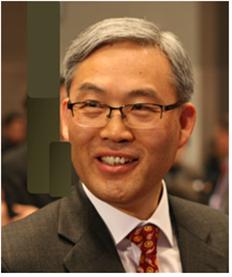 Professor Chun-Taek Rim Appointed as Associate Editor for IEEE TPEL
Professor Chun-Taek Rim of the nuclear and quantum engineering at KAIST was appointed as an associate editor of the Institute of Electrical and Electronics Engineers (IEEE) Transactions on Power Electronics (TPEL), an eminent academic journal bio-monthly published in the field of power electronics.The journal has a high impact factor (4.08), a measure reflecting the average number of citations to recent articles published in an academic journal, which ranks as the 6th the most influential journal among the 100 journals published by IEEE.Professor Rim was also appointed to an associate editor for IEEE Journal of Emerging and Selected Topics in Power Electronics in September in recognition of his expertise in wireless power and electric vehicles.
2013.11.15 View 12788
Professor Chun-Taek Rim Appointed as Associate Editor for IEEE TPEL
Professor Chun-Taek Rim of the nuclear and quantum engineering at KAIST was appointed as an associate editor of the Institute of Electrical and Electronics Engineers (IEEE) Transactions on Power Electronics (TPEL), an eminent academic journal bio-monthly published in the field of power electronics.The journal has a high impact factor (4.08), a measure reflecting the average number of citations to recent articles published in an academic journal, which ranks as the 6th the most influential journal among the 100 journals published by IEEE.Professor Rim was also appointed to an associate editor for IEEE Journal of Emerging and Selected Topics in Power Electronics in September in recognition of his expertise in wireless power and electric vehicles.
2013.11.15 View 12788 -
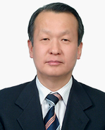
 Professor Hwang Gyu Young Elected as Chairman of IEEE TCDE.
Professor Hwang Gyu Young (Department of Computer Science) was elected as the Chairman of IEEE (Institute of Electrical and Electronics Engineers) TCDE (Technical Committee on Data Engineering).
IEEE TCDE is one of the three academic organizations (including VLDB Endowment, ACM SIGMOD) and Professor Hwang is the first to be elected as Chairman from the Asia-Pacific region.
Professor Hwang’s tenure begins on New Year’s Day for two years.
IEEE TCDE holds the world’s most prestigious academic competition IEEE ICDE and hosts the Working Group and publishes the IEEE Data Engineering Bulletin.
2012.12.21 View 12173
Professor Hwang Gyu Young Elected as Chairman of IEEE TCDE.
Professor Hwang Gyu Young (Department of Computer Science) was elected as the Chairman of IEEE (Institute of Electrical and Electronics Engineers) TCDE (Technical Committee on Data Engineering).
IEEE TCDE is one of the three academic organizations (including VLDB Endowment, ACM SIGMOD) and Professor Hwang is the first to be elected as Chairman from the Asia-Pacific region.
Professor Hwang’s tenure begins on New Year’s Day for two years.
IEEE TCDE holds the world’s most prestigious academic competition IEEE ICDE and hosts the Working Group and publishes the IEEE Data Engineering Bulletin.
2012.12.21 View 12173 -
2012 Intellectual Property Rights Award Ceremony Held
The 2012 Intellectual Property Rights Award Ceremony was held at Seoul KAIST Campus.
Recipients of the award included former congressmen Kim Young Sun and Lee Jeong Hyuk, and Kim Boo Kyung researcher at Electronics and Telecommunications Research Institute also representing Vooz Ltd. that created the character POOCA.
The Intellectual Property Rights Award is given to an individual or a group that succeeded in utilizing, protecting, creating, and establishment of its foundation including patent, copyright, and brand. Intellectual Property Rights is viewed as of importance for future national competitiveness.
The Award is organized by the Korea Patent Attorneys Association, the Korea Association of Intellectual Property Services, and KAIST and are respectively core institutions in the training of Intellectual Property Rights Experts and the creation, utilization, and the protection of intellectual property.
In addition the Award is also co-organized by the KAIST Graduate School of Intellectual Property Rights (established in cooperation with KAIST and the Korean Intellectual Property Office) and the total 20 million Won of prize money is funded by Korea Institute of Intellectual Strategy and Kim Ok Lan Foundation.
The Award Ceremony was held with a special lecture by the recipients.
It was stressed that the evaluation process was carried out with that the decision is a silent message to the society and is also a type of market signal.
Director Ko Gi Seok (Presidential Council on Intellectual Property) revealed that the candidates’ impact on the strength of national intellectual property rights was thoroughly scrutinized.
In the criteria of Creation of Intellectual Property, ETRI received the award in recognition of the institution’s successful patenting and commercializing of products of Korean R&D.
ETRI created a total of 251 International Patents in cooperation with ITU, ISO, IEE, etc. and also participated in a total of 9 International Standard Patent Pool, showing its active Intellectual Property management.
Such efforts ranked ETRI 1st in the United States Patent Evaluation performed by the US Patent Board in 2011 out of 237 institutions.
In addition Recipient of the Intellectual Property Utilization criteria, VOOZ ltd.’s Kim Boo Kyung promised the free use of their character POOCA in ETRI’s automated Korean-English translator. Researcher Kim Boo Kyung was rewarded with the award in recognition of his contribution to the domestic economy and realization of the commercialization of a copy right through licensing.
Former congressman Kim Young Son received an Award in the Foundation criteria in recognition of his efforts in the establishment of the Presidential Council on Intellectual Property and the Basic Blueprints for the Intellectual Property Law.
Former congressman Lee Jeong Hyuk received the same award in recognition of standardization and streamlining Intellectual Property Rights Policies. His realization and pursuit of the establishment of a balanced growth based on law for the competitiveness of businesses was the driving force behind his accomplishments.
2012.10.16 View 13931
-
 KAIST researchers verify and control the mechanical properties of graphene
KAIST researchers have successfully verified and controlled the mechanical properties of graphene, a next-generation material. Professor Park Jung Yong from the EEWS Graduate School and Professor Kim Yong Hyun from the Graduate School of Nanoscience and Technology have succeeded in fluorinating a single atomic-layered graphene sample and controlling its frictional and adhesive properties. This is the first time the frictional properties of graphene have been examined at the atomic level, and the technology is expected to be applied to nano-sized robots and microscopic joints.
Graphene is often dubbed “the dream material” because of its ability to conduct high amounts of electricity even when bent, making it the next-generation substitute for silicon semiconductors, paving the way for flexible display and wearable computer technologies. Graphene also has high potential applications in mechanical engineering because of its great material strength, but its mechanical properties remained elusive until now.
Professor Park’s research team successfully produced individual graphene samples with fluorine-deficiency at the atomic level by placing the samples in Fluoro-xenon (XeF2) gas and applying heat. The surface of the graphene was scanned using a micro probe and a high vacuum atomic microscope to measure its dynamic properties.
The research team found that the fluorinated graphene sample had 6 times more friction and 0.7 times more adhesiveness than the original graphene. Electrical measurements confirmed the fluorination process, and the analysis of the findings helped setup the theory of frictional changes in graphene.
Professor Park stated that “graphene can be used for the lubrication of joints in nano-sized devices” and that this research has numerous applications such as the coating of graphene-based microdynamic devices.
This research was published in the online June edition of Nano Letters and was supported by the Ministry of Science, Technology, and Education and the National Research Foundation as part of the World Class University (WCU) program.
2012.07.24 View 19453
KAIST researchers verify and control the mechanical properties of graphene
KAIST researchers have successfully verified and controlled the mechanical properties of graphene, a next-generation material. Professor Park Jung Yong from the EEWS Graduate School and Professor Kim Yong Hyun from the Graduate School of Nanoscience and Technology have succeeded in fluorinating a single atomic-layered graphene sample and controlling its frictional and adhesive properties. This is the first time the frictional properties of graphene have been examined at the atomic level, and the technology is expected to be applied to nano-sized robots and microscopic joints.
Graphene is often dubbed “the dream material” because of its ability to conduct high amounts of electricity even when bent, making it the next-generation substitute for silicon semiconductors, paving the way for flexible display and wearable computer technologies. Graphene also has high potential applications in mechanical engineering because of its great material strength, but its mechanical properties remained elusive until now.
Professor Park’s research team successfully produced individual graphene samples with fluorine-deficiency at the atomic level by placing the samples in Fluoro-xenon (XeF2) gas and applying heat. The surface of the graphene was scanned using a micro probe and a high vacuum atomic microscope to measure its dynamic properties.
The research team found that the fluorinated graphene sample had 6 times more friction and 0.7 times more adhesiveness than the original graphene. Electrical measurements confirmed the fluorination process, and the analysis of the findings helped setup the theory of frictional changes in graphene.
Professor Park stated that “graphene can be used for the lubrication of joints in nano-sized devices” and that this research has numerous applications such as the coating of graphene-based microdynamic devices.
This research was published in the online June edition of Nano Letters and was supported by the Ministry of Science, Technology, and Education and the National Research Foundation as part of the World Class University (WCU) program.
2012.07.24 View 19453 -
New wireless charging device developed
The On-line Electric Vehicle (OLEV) developed by KAIST has made a step towards commercialization with the development of a more economic wireless charging device.
Professor Chun-Taek Rim from the Department of Nuclear and Quantum Engineering at KAIST has developed a new I-shaped wireless charging device that differs from the pre-existing rail-type electricity feeder. This device can be modularly produced and requires relatively less construction, significantly reducing the cost of implementation.
The KAIST OLEV is a new concept electric car that has a special electricity collecting device underneath it. The car’s battery is charged by magnetic fields produced from electric lines buried 15cm underneath the road. The vehicle was first tested in 2009, making it the first wireless electric car in the world. OLEV can be charged during stoppage time between traffic lights and receives real-time power when running. OLEV is currently in operation at the KAIST Munji Campus in Daejeon and is also being exhibited at the Yeosu Expo and Seoul Grand Park.
The device itself has a charging capacity of 15kW, and the electricity is supplied through an electricity feeder with a width of 80cm with a space interval of 20cm. Despite being hailed as a technological breakthrough and revolutionary concept, KAIST OLEV has been criticized for problems in commercialization, due to the difficulties in installing wires beneath existing roads, which costs a considerable amount of money.
The new I-shaped wireless charging device reduces the width of the electricity feeder by 10cm, a mere one-eighth of the size of the previous version, and greatly increases the charging power to 25kW. Furthermore, the left and right permissible space of automobiles has increased to 24cm and the magnetic field complies with the international design guidelines, making the OLEV safe for the human body.
The reduction of the width has made the mass production of modules possible, making the installation of KAIST OLEV more economical and marketable. Professor Rim emphasized that compared with the existing rail-type electricity feeder, the new technology will need only one-tenth of the construction time and 80% of the cost, significantly improving OLEV’s constructability and workability.
The research was published in the IEEE Transactions on Power Electronics last December, and Professor Rim was invited to talk at the Conference on Electric Roads & Vehicles, which was held in February in the United States, about the new technology.
2012.07.06 View 13724
-
A Step Closer to Ultra Slim Mobile Phone
Professor Baek Kyung Wook (department of Material Science and Engineering) succeeded in developing an ultra-thin conjugation technique that can perfectly replace the modular contact in electronic devices.
The research team developed a compound material using ultra-fine solder-adhesive film and developed the vertical ultrasonic conjugation process thereby making a reliable utra-thin conjugation.
The developed technique allowed for very thin and reliable conjugation and will be able to replace the socket type connector and is expected to revolutionize the electronic device industry.
In mobile electronic devices like the smartphone, the trend is to incorporate various functional modules like camera, display, touchscreens, etc. in addition to striving for miniaturization of the device.
Recently the problem was the fact that the number of modules within the device was increasing due to the incorporation of various functions, and consequently the volume that these modules took up increased as well, which made miniaturization almost impossible.
Professor Baek‘s team succeeded in improving upon this problem by creating a compound material that has ultra-fine solder particles that can melt to form alloy fusion with the electrode and thermosetting adhesive film that can wrap around the electrode and provide mechanical protection.
The use of this material made it possible to reduce the thickness of the connector by hundredth fold which improved electrical, mechanical properties and highly reliable.
From a processing standpoint the conventional conjugation process involved heating the mechanical block and was therefore hard to manage its production and also consumed 1000W and took up to 15 seconds.
By contrast, Professor Baek’s team’s new process uses only ultrasound to locally heat and melt the conjugation point itself thereby reducing power consumption to 100W and conjugation time to 1~5 seconds.
The technique developed by Professor Baek and Lee Ki Won Doctorate student was awarded Excellent Dissertation Award by world famous journals like the Electronic Components and Technology Conference and is being recognized worldwide.
2012.01.31 View 12036
-
'WWW2014' to be held in Seoul
WWW2014 (World Wide Web 2014) will be held in Seoul.
KAIST, Agency for Technology and Standards, W3C (World Wide Web Consortium), and ETRI (Electronics and Telecommunications Research Institute) all worked in cooperation to have WWW2014 in Seoul. The announcement that WWW2014 will be held in Seoul was announced in the Closing Ceremony of WWW2011 India Conference. Seoul overtook Adelaide and Melbourne of Australia.
Hosting WWW2014 in Seoul will be a great opportunity to showcase Korea’s Web Technology and get a grasp on the current trend in the field of high tech web technology and services.
The WWW conferences are attended by over 1,000 experts all over the world and are the world’s largest international conference in the field of IT.
Efforts to host the conference in their own respective countries are made on a national scale. The WWW2011 was hosted in India with the President of India giving an opening ceremony speech and WWW2013 will be hosted in Brazil in part due to the President himself sending a letter to express their desire to host WWW conference.
2011.05.11 View 13095
-
A Light Weight, Energy Effcient Household Polysomnography (PSG) System Developed
A smart ‘household polysomnography (PSG) system’ was developed by domestic research team.
Professor Yoo Hui Joon and his research team of KAIST’s department of Electricity and Electronic Engineering successfully developed a PSG system that is light weight and has high performance levels. The conventional PSG systems were complex with numerous lines and wires.
The PSG is used to monitor biological signals during sleep and the monitored results are used to diagnose and cure sleep-related illnesses and disorders. However because of restrictions like the size of the machine, impurities, and the change in environment, multiple trials over several days were required to obtain accurate data.
The system developed by the research team is lighter than a q-tip so as to not disturb the patient’s sleep. It also has Intelligent Circuit (IC) that detects when sensors come detached and automatically replaces the sensor with another sensor thereby allowing continual monitoring of the user.
A low-power consuming circuit was implemented allowing the entire system to run continuously on a single coin battery for 10 hours which effectively decreased the weight of the system and simultaneously allows for uninterrupted monitoring of the user over the entire sleep cycle.
Even a remote diagnosis system can be implemented. The user will don the PSG and sleep at home, ensuring that a normal heat beat rate, brain waves, breathing, etc. will be monitored. The data procured overnight can be sent to the experts online who will be able to diagnose remotely.
The research team plans on performing research in cooperation with the KAIST hospital and U-Healthcare research.
The research result is winning worldwide rave. The system was announced in the International Solid-State Circuits Conference (ISSCC) and was published in ISSCC magazine and in Japan’s NIKKEI Electronics January edition.
2011.03.25 View 14802
-
 Former Minister of Information & Communications Dae-Je Jin donated to KAIST.
From left to right: Yong-Hoo Lee, Dean of Information Science & Technology College, KAIST; Gang-Seok Lee, Vice President of Skylake Incuvest, Inc.; Dae-Je Jin, Former Minister of Information & Communications; Byung-Kyu Choi, Provost of KAIST; and Dae-Joon Joo, Vice President of Planning & Budget, KAIST.
Mr. Dae-Je Jin, who had served as the Minister of Information & Communications, South Korea, gave away about 100,000 USD to KAIST and hoped that his donation would be used for the development of information and technology industry in the nation.
Mr. Jin, widely known as one of the reputable business leaders in the IT industry, was also once the president of Samsung Electronics, a leading global supplier of electronic products and goods. Currently, he runs a private equity investor called, Skylake Incuvest, Inc., which invests and incubates innovative information, communications, and technology companies.
“The real growth engine for our nation to become an economic powerhouse on a global stage has been the highly trained people who shore up our industry. Universities including KAIST have played an excellent role in providing our nation with such outstanding researchers and engineers. I will continue to support for KAIST"s mission as a leading research university in science and technology in Korea and the world,” said Mr. Jin.
KAIST said that his donation would be used for the support of its IT researches.
2010.08.27 View 14006
Former Minister of Information & Communications Dae-Je Jin donated to KAIST.
From left to right: Yong-Hoo Lee, Dean of Information Science & Technology College, KAIST; Gang-Seok Lee, Vice President of Skylake Incuvest, Inc.; Dae-Je Jin, Former Minister of Information & Communications; Byung-Kyu Choi, Provost of KAIST; and Dae-Joon Joo, Vice President of Planning & Budget, KAIST.
Mr. Dae-Je Jin, who had served as the Minister of Information & Communications, South Korea, gave away about 100,000 USD to KAIST and hoped that his donation would be used for the development of information and technology industry in the nation.
Mr. Jin, widely known as one of the reputable business leaders in the IT industry, was also once the president of Samsung Electronics, a leading global supplier of electronic products and goods. Currently, he runs a private equity investor called, Skylake Incuvest, Inc., which invests and incubates innovative information, communications, and technology companies.
“The real growth engine for our nation to become an economic powerhouse on a global stage has been the highly trained people who shore up our industry. Universities including KAIST have played an excellent role in providing our nation with such outstanding researchers and engineers. I will continue to support for KAIST"s mission as a leading research university in science and technology in Korea and the world,” said Mr. Jin.
KAIST said that his donation would be used for the support of its IT researches.
2010.08.27 View 14006 -
Master of Science in Intellectual Property: First Class Starts on Saturday, February 6, 2010
Newly Established, Postgraduate Course for Master of Science in Intellectual Property
First class starts on February 6th, 2010
In conjunction with Korean Intellectual Property Office (KIPO), KAIST has established a new postgraduate course for a master of science in intellectual property (IP). 41 students have enrolled the course, and its first class will begin February 6th, 2010. With a diverse professional background, the first-year students came from private businesses, IP service industry, and public organizations.
Globally well-known companies—Samsung Electronics, LG Electronics, and the Pohang Iron and Steel Company (POSCO)—and mid-sized companies have offered scholarships to support the new M.S. Program. Business and industry in Korea have recognized the increasingly important role of intellectual property in a modern economy and showed a strong interest in developing workforce specialized in subjects such as, but not limited to, patent law, copyright and designs law, trade mark law, unfair competition, anti-trust law, competition law, and trade secret law.
Prosecutor Chan-Gi Na from Seoul Central District Prosecutor’s Office said, “I’ve applied for the master program at KAIST because I wanted to learn more about intellectual property in greater depth. Through the coursework, I hope to enhance my knowledge on the subjects and use it for the protection of Koreans’ IP related rights and the development of our nation’s IP industry.”
Assistant Manager Jin-Hong Bae from Samsung Securities, Inc. said, “Since the capital market law becomes effective, the need for developing new financial products or services in our finance market has rapidly grown. We no longer can make our financial products by simply copying or ripping off ideas from others. It’s a must practice, not an option, to set up a system under which we are able to protect our IPs.”
“I would like to become an expert in our finance market, who really knows how to commercialize intellectual property assets into benefits, so any know-hows or ideas accumulated from years of working in the field can be registered and protected,” added Mr. Bae.
KAIST’s Mater Program for intellectual property is designed for engineers who wish to acquire the skills required to play a leading role in the field. These engineers, KAIST anticipates, will establish and execute business strategies to protect intellectual property, generate added values for a company, and effectively respond against patent related claims.
The intellectual property will seize up to 90% of business values to be generated in the 21st century. KAIST has long foreseen the need for training top-notch engineers in intellectual property. Combined with multidisciplinary approach to engineering, law, and management, the new M.S. Program will provide students with a variety form of classes to assist them in getting a practical knowledge as needed based on their interests and career aspirations. Examples of the classes are workshops on the change in technology trends—i.e., information technology (IT), environmental technology (ET), and bio technology (BT); standardization of intellectual property and value assessment; and patent law related claims.
“All professors involved in the course are experts who are equipped with hands-on experiences in working on intellectual property for a long time at government agencies, companies, and law firms,” Professor Chul-Ho Kim, responsible for overseeing the entire program, said.
He also expressed his confidence that “We have set up an academic system to induct highly qualified professionals and engineers, capable of handling all aspects of intellectual property related issues, into work places. Our coursework encompasses technology, research and development (R&D), and management, and students who complete the program will be ready to tackle down any intellectual property matters in the 21st century.”
Freshmen convocation for the IP M.S. Program is scheduled on February 20th at KAIST, and President Nam Pyo Suh and Commissioner Jung-Sik Koh of Korean Intellectual Property (KIPO) will attend the event.
2010.02.04 View 16521
-
 Prof. Yu Wins Sidney Stein International Award
Prof. Jin Yu of the Department of Materials Science and Engineering won the Sidney J. Stein International Award at the plenary session of the International Microelectronics and Packaging Society (IMAPS) held in San Jose, the United States, on Nov. 3.
The Sidney Stein International Award recognizes an individual who is regarded as providing significant international technical and/or leadership contributions to the microelectronics packaging industry, while participating and demonstrating support of IMAPS international activities to enhance the electronics packaging profession.
The International Microelectronics And Packaging Society is the largest society dedicated to the advancement and growth of microelectronics and electronics packaging. It offers chapters around the globe, creating global networks of more than 4,000 members in the United States and an additional 4,000 members throughout Europe and Asia. Prof. Yu currently serves as the chairman of its Asia League Chapter and the Korean Microelectronics and Packaging Society.
2009.11.20 View 15877
Prof. Yu Wins Sidney Stein International Award
Prof. Jin Yu of the Department of Materials Science and Engineering won the Sidney J. Stein International Award at the plenary session of the International Microelectronics and Packaging Society (IMAPS) held in San Jose, the United States, on Nov. 3.
The Sidney Stein International Award recognizes an individual who is regarded as providing significant international technical and/or leadership contributions to the microelectronics packaging industry, while participating and demonstrating support of IMAPS international activities to enhance the electronics packaging profession.
The International Microelectronics And Packaging Society is the largest society dedicated to the advancement and growth of microelectronics and electronics packaging. It offers chapters around the globe, creating global networks of more than 4,000 members in the United States and an additional 4,000 members throughout Europe and Asia. Prof. Yu currently serves as the chairman of its Asia League Chapter and the Korean Microelectronics and Packaging Society.
2009.11.20 View 15877 -
 Prof. Park to Receive HP's Annual Innovation Research Award
Prof. In-Kyu Park of the Department of Mechanical Engineering, KAIST, has been will receive an award from Hewlett-Packard"s second annual Labs Innovation Research Program, university authorities said on Wednesday (July 8).
Prof. Park was chosen as the winner of the research award for his paper entitled "Eco-friendly nanomanufacturing for intelligent environment sensing applications."
Sixty projects from 46 universities in 12 countries were selected as the recipients of the awards from HP Labs, the company"s central research arm. The program is designed to create opportunities for colleges, universities and research institutes to conduct collaborative research with HP.
HP Labs Innovation Research Awards provide project funding of up to $100,000 for one year to each of the chosen academic institutions, which is renewable for up to three years based on research progress and HP business requirements.
Prof. Park has conducted joint researches on nanoimprinting, nanosensors, and nanoelectronics with HP"s Information and Quantum Systems Lab since 2005. Starting from the later half of 2009, he is to receive research grants under the industry-academia cooperation program of the world"s information technology giant firm.
2009.07.09 View 18576
Prof. Park to Receive HP's Annual Innovation Research Award
Prof. In-Kyu Park of the Department of Mechanical Engineering, KAIST, has been will receive an award from Hewlett-Packard"s second annual Labs Innovation Research Program, university authorities said on Wednesday (July 8).
Prof. Park was chosen as the winner of the research award for his paper entitled "Eco-friendly nanomanufacturing for intelligent environment sensing applications."
Sixty projects from 46 universities in 12 countries were selected as the recipients of the awards from HP Labs, the company"s central research arm. The program is designed to create opportunities for colleges, universities and research institutes to conduct collaborative research with HP.
HP Labs Innovation Research Awards provide project funding of up to $100,000 for one year to each of the chosen academic institutions, which is renewable for up to three years based on research progress and HP business requirements.
Prof. Park has conducted joint researches on nanoimprinting, nanosensors, and nanoelectronics with HP"s Information and Quantum Systems Lab since 2005. Starting from the later half of 2009, he is to receive research grants under the industry-academia cooperation program of the world"s information technology giant firm.
2009.07.09 View 18576