NT
-
 Professor Haeng-Ki Lee appointed as "ICCES Distinguished Fellow"
Professor Haeng-Ki Lee
Professor Haeng-Ki Lee from the Department of Civil and Environmental Engineering at KAIST has been appointed as “Distinguished Fellow” and has also received the “Outstanding Research Award” at the International Conference on Computational & Experimental Engineering and Sciences (ICCES).
Founded in 1986, ICCES is regarded as one of the most prestigious international conferences in the field of computational mechanics and experimental engineering.
The Nominating Committee at ICCES recommends the appointment of a distinguished member who has made significant contributions to the development of computational mechanics and experimental engineering. Professor Lee was the first Korean who received such title. Furthermore, he was the recipient of the “Outstanding Research Award” presented by ICCES for his academic research on damage mechanics of complex systems.
Professor Lee is currently serving as the Head of the Department of Civil and Environmental Engineering at KAIST and the Director of BK Plus Agency, a Korean government’s research program. He received an award from the Minister of Science, ICT and Future Planning in 2013 for the promotion of science and technology.
2014.07.02 View 14086
Professor Haeng-Ki Lee appointed as "ICCES Distinguished Fellow"
Professor Haeng-Ki Lee
Professor Haeng-Ki Lee from the Department of Civil and Environmental Engineering at KAIST has been appointed as “Distinguished Fellow” and has also received the “Outstanding Research Award” at the International Conference on Computational & Experimental Engineering and Sciences (ICCES).
Founded in 1986, ICCES is regarded as one of the most prestigious international conferences in the field of computational mechanics and experimental engineering.
The Nominating Committee at ICCES recommends the appointment of a distinguished member who has made significant contributions to the development of computational mechanics and experimental engineering. Professor Lee was the first Korean who received such title. Furthermore, he was the recipient of the “Outstanding Research Award” presented by ICCES for his academic research on damage mechanics of complex systems.
Professor Lee is currently serving as the Head of the Department of Civil and Environmental Engineering at KAIST and the Director of BK Plus Agency, a Korean government’s research program. He received an award from the Minister of Science, ICT and Future Planning in 2013 for the promotion of science and technology.
2014.07.02 View 14086 -
 A KAIST startup, YBrain, builds a wearable device to cure Alzheimer's
A group of KAIST graduates from the Departments of Bio and Brain Engineering, Computer Science, Materials Science Engineering, and Industrial Design created a startup called YBrain (http://ybrain.com/). YBrain develops a wearable neuroscience technology to treat or reduce the symptoms of degenerative brain diseases such as dementia and Alzheimer’s. Their recent technological developments were covered in e27, one of the leading blogs based in Singapore. The blog covers topics like the latest technology innovation, startups, and entrepreneurship in Asia. A news article follows below:
e27, June 24, 2014
“This wearable tech may be able to combat effects of Alzheimer’s”
http://e27.co/this-wearable-tech-may-be-able-combat-effects-of-alzheimers-20140624/
2014.06.25 View 14779
A KAIST startup, YBrain, builds a wearable device to cure Alzheimer's
A group of KAIST graduates from the Departments of Bio and Brain Engineering, Computer Science, Materials Science Engineering, and Industrial Design created a startup called YBrain (http://ybrain.com/). YBrain develops a wearable neuroscience technology to treat or reduce the symptoms of degenerative brain diseases such as dementia and Alzheimer’s. Their recent technological developments were covered in e27, one of the leading blogs based in Singapore. The blog covers topics like the latest technology innovation, startups, and entrepreneurship in Asia. A news article follows below:
e27, June 24, 2014
“This wearable tech may be able to combat effects of Alzheimer’s”
http://e27.co/this-wearable-tech-may-be-able-combat-effects-of-alzheimers-20140624/
2014.06.25 View 14779 -
 KAIST doctoral student wins prize at 2014 International Military Science and Technology Fair
Min-Kyu Yoo (far left), a doctoral student in the Department of Materials Science Engineering, KAIST, received a silver prize at the 2014 International Military Science and Technology Fair held from May 29 to June 1, 2014 at KINTEX, Ilsan City, Korea.
Yoo presented a paper on aluminum composite materials that were reinforced by carbon nanotubes. Carbon nanotubes reinforced aluminum composite materials have strong mechanical properties, and some nations have used them to manufacture battle tanks.
Aluminum generates hydrogen in an alkaline solution. Utilizing this property and the galvanic corrosion of carbon nanotubes and aluminums, Yoo developed a hydrogen energy system that is fueled with composite materials of carbon nanotube reinforced aluminum. He produced 5 kW electric power and maintained it 22 days using 10 kg of the composite materials for a proton exchange membrane fuel cell and its auxiliary power system.
Yoo’s research will alleviate the difficulty of transporting fuels during wartime and can be applied to the development of an auxiliary power system for next generation aircrafts and battle tanks.
2014.06.24 View 11047
KAIST doctoral student wins prize at 2014 International Military Science and Technology Fair
Min-Kyu Yoo (far left), a doctoral student in the Department of Materials Science Engineering, KAIST, received a silver prize at the 2014 International Military Science and Technology Fair held from May 29 to June 1, 2014 at KINTEX, Ilsan City, Korea.
Yoo presented a paper on aluminum composite materials that were reinforced by carbon nanotubes. Carbon nanotubes reinforced aluminum composite materials have strong mechanical properties, and some nations have used them to manufacture battle tanks.
Aluminum generates hydrogen in an alkaline solution. Utilizing this property and the galvanic corrosion of carbon nanotubes and aluminums, Yoo developed a hydrogen energy system that is fueled with composite materials of carbon nanotube reinforced aluminum. He produced 5 kW electric power and maintained it 22 days using 10 kg of the composite materials for a proton exchange membrane fuel cell and its auxiliary power system.
Yoo’s research will alleviate the difficulty of transporting fuels during wartime and can be applied to the development of an auxiliary power system for next generation aircrafts and battle tanks.
2014.06.24 View 11047 -
 KAIST's Center for Integrated Smart Sensors made a partnership with a Silicon Valley start-up
KAIST's Center for Integrated Smart Sensors (CISS) will implement a joint venture project with Dual Aperture, Inc., a leading digital camera provider based in Palo Alto, California. The two will work on the development of 3-D imaging technology.
CISS, headed by Professor Chong-Min Kyung of Electrical Engineering, KAIST, is dedicated to technological advancement by developing innovative devices, circuits, and smart sensors.
In its press release dated June 18, 2014, Dual Aperture, Inc. stated that “by combining top talents in engineering, the partnership will establish a groundbreaking smart sensor technology accessible on multiple platforms and devices.”
For details, a Fox news article follows below:
Dual Aperture, Inc., June 18, 2014
“Image technology leader and top research institute collaborate engineering resources to create world’s first-ever smart sensor technology”
http://www.fox14tv.com/story/25808022/dual-aperture-announces-joint-venture-with-kaists-center-for-integrated-smart-sensors
2014.06.19 View 10954
KAIST's Center for Integrated Smart Sensors made a partnership with a Silicon Valley start-up
KAIST's Center for Integrated Smart Sensors (CISS) will implement a joint venture project with Dual Aperture, Inc., a leading digital camera provider based in Palo Alto, California. The two will work on the development of 3-D imaging technology.
CISS, headed by Professor Chong-Min Kyung of Electrical Engineering, KAIST, is dedicated to technological advancement by developing innovative devices, circuits, and smart sensors.
In its press release dated June 18, 2014, Dual Aperture, Inc. stated that “by combining top talents in engineering, the partnership will establish a groundbreaking smart sensor technology accessible on multiple platforms and devices.”
For details, a Fox news article follows below:
Dual Aperture, Inc., June 18, 2014
“Image technology leader and top research institute collaborate engineering resources to create world’s first-ever smart sensor technology”
http://www.fox14tv.com/story/25808022/dual-aperture-announces-joint-venture-with-kaists-center-for-integrated-smart-sensors
2014.06.19 View 10954 -
 Professor Sang Ouk Kim Receives the "Scientist of the Month Award" from the Korean Government
Professor Sang Ouk Kim of the Department of Materials Science and Engineering, KAIST, received the Scientist of the Month Award in June 2014 for his development of a fundamental technology that allows free control of the properties of carbon-based materials.
Since June 1997, the Korean government has awarded monthly one scientist working in industry, universities, or research institutions to recognize his or her research achievements, as well as to promote science and technology.
Professor Kim implemented a technique known as doping, which has been used in ordinary semiconductor processes, to demonstrate the physical properties of carbon-based materials. Carbon nanotubes, graphene, and other carbon materials have superior mechanical and electrical properties and are regarded as next-generation materials. However, difficulty in controlling their qualities has made applications in various devices unfavorable. The doping technique in semiconductor production is to artificially introduce impurities into an extremely pure semiconductor for the purpose of modulating its electrical properties.
Profess Kim doped elements like nitrogen and boron to enable minute control of the physical properties of carbon-based materials and applied the technique to development of organic solar cells, organic light-emitting devices, and flexible memory. He also increased the application range by using a self-assembly method to change freely the structure of carbon-based materials.
Professor Kim has published 53 papers in renowned journals such as Advanced Materials and Nanoletters. He was rewarded further by being invited to write a review paper for the 25th anniversary special edition for Advanced Materials.
2014.06.19 View 12247
Professor Sang Ouk Kim Receives the "Scientist of the Month Award" from the Korean Government
Professor Sang Ouk Kim of the Department of Materials Science and Engineering, KAIST, received the Scientist of the Month Award in June 2014 for his development of a fundamental technology that allows free control of the properties of carbon-based materials.
Since June 1997, the Korean government has awarded monthly one scientist working in industry, universities, or research institutions to recognize his or her research achievements, as well as to promote science and technology.
Professor Kim implemented a technique known as doping, which has been used in ordinary semiconductor processes, to demonstrate the physical properties of carbon-based materials. Carbon nanotubes, graphene, and other carbon materials have superior mechanical and electrical properties and are regarded as next-generation materials. However, difficulty in controlling their qualities has made applications in various devices unfavorable. The doping technique in semiconductor production is to artificially introduce impurities into an extremely pure semiconductor for the purpose of modulating its electrical properties.
Profess Kim doped elements like nitrogen and boron to enable minute control of the physical properties of carbon-based materials and applied the technique to development of organic solar cells, organic light-emitting devices, and flexible memory. He also increased the application range by using a self-assembly method to change freely the structure of carbon-based materials.
Professor Kim has published 53 papers in renowned journals such as Advanced Materials and Nanoletters. He was rewarded further by being invited to write a review paper for the 25th anniversary special edition for Advanced Materials.
2014.06.19 View 12247 -
 Professor Sung Yong Kim Appointed as Committee Member to Serve PICES
The Pacific International Council for the Exploration of the Sea: North Pacific Marine Science Organization (PICES) is an intergovernmental organization, which was established in 1992 to promote and coordinate marine research in the North Pacific and adjacent areas. Currently, the United States, Canada, Japan, China, Russia, and Korea are members of the organization.
Professor Sung Yong Kim of Ocean Systems Engineering, KAIST, has been appointed to serve the Scientific and Technical Committees of PICES. He will begin his stint from July 1, 2014. During his assignment, Professor Kim will identify the need for observation of the North Pacific marine environment, develop observation methodology, and publish an annual report on the observation.
Professor Kim is an expert in marine physics and environmental fluids, with a focus on coastal circulation and dynamics, mesoscale and submesoscale eddies, integrated coastal ocean observing system, and statistical and dynamic data analysis.
2014.06.18 View 10998
Professor Sung Yong Kim Appointed as Committee Member to Serve PICES
The Pacific International Council for the Exploration of the Sea: North Pacific Marine Science Organization (PICES) is an intergovernmental organization, which was established in 1992 to promote and coordinate marine research in the North Pacific and adjacent areas. Currently, the United States, Canada, Japan, China, Russia, and Korea are members of the organization.
Professor Sung Yong Kim of Ocean Systems Engineering, KAIST, has been appointed to serve the Scientific and Technical Committees of PICES. He will begin his stint from July 1, 2014. During his assignment, Professor Kim will identify the need for observation of the North Pacific marine environment, develop observation methodology, and publish an annual report on the observation.
Professor Kim is an expert in marine physics and environmental fluids, with a focus on coastal circulation and dynamics, mesoscale and submesoscale eddies, integrated coastal ocean observing system, and statistical and dynamic data analysis.
2014.06.18 View 10998 -
 Professor Sang-Ouk Kim's Research on Carbon Materials Featured in a Philippines Science News
The subject article said that Professor Sang-Ouk Kim of Materials Science Engineering at KAIST “developed a technique to change the nature of the next-generation carbon-based materials. His research has expanded the possibility of carbon-based materials to be used in clothes.”
For details, please refer to the article below:
Centrio Times, June 10, 2014
KAIST scientist develops color changing carbon materials that can be used in clothes
http://www.centriotimes.com/2014/06/kaist-scientist-develops-color-changing-carbon-materials-can-used-clothes.html.
2014.06.15 View 9611
Professor Sang-Ouk Kim's Research on Carbon Materials Featured in a Philippines Science News
The subject article said that Professor Sang-Ouk Kim of Materials Science Engineering at KAIST “developed a technique to change the nature of the next-generation carbon-based materials. His research has expanded the possibility of carbon-based materials to be used in clothes.”
For details, please refer to the article below:
Centrio Times, June 10, 2014
KAIST scientist develops color changing carbon materials that can be used in clothes
http://www.centriotimes.com/2014/06/kaist-scientist-develops-color-changing-carbon-materials-can-used-clothes.html.
2014.06.15 View 9611 -
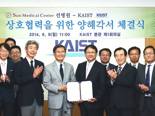 MOU between KAIST and Sun Medical Center on "Mobile Health Care"
KAIST and Sun Medical Center signed a memorandum of understanding (MOU) in front of 20 attendees including KAIST President Steve Kang and Sun Medical Center Director Seung-Hoon Sun on June 9 at KAIST to expand medical services through medical and electronic telecommunication technology.
The two organizations will cooperate on the research and development of mobile healthcare, systems for the medical industry, remote medical treatment for overseas patients, and working toward improving national healthcare. The two parties will also develop wearable devices and mobile sensors which will become a welcome addition to the global healthcare market.
KAIST President Steve Kang explained, “With Sun Medical Center’s 50 years of experience in medical technology and KAIST’s World University Ranking of 20th in information technology, a new brainchild in the mobile healthcare field will be produced.”
In the meantime, KAIST’s College of Information Science and Technology is making developments in mobile healthcare systems which can accumulate medical information and apply it to medical services by using personal bio-information data. Ambitious new projects are underway, such as the “Dr. M Project“ which launched in March with 28 full-time researchers.
2014.06.14 View 8721
MOU between KAIST and Sun Medical Center on "Mobile Health Care"
KAIST and Sun Medical Center signed a memorandum of understanding (MOU) in front of 20 attendees including KAIST President Steve Kang and Sun Medical Center Director Seung-Hoon Sun on June 9 at KAIST to expand medical services through medical and electronic telecommunication technology.
The two organizations will cooperate on the research and development of mobile healthcare, systems for the medical industry, remote medical treatment for overseas patients, and working toward improving national healthcare. The two parties will also develop wearable devices and mobile sensors which will become a welcome addition to the global healthcare market.
KAIST President Steve Kang explained, “With Sun Medical Center’s 50 years of experience in medical technology and KAIST’s World University Ranking of 20th in information technology, a new brainchild in the mobile healthcare field will be produced.”
In the meantime, KAIST’s College of Information Science and Technology is making developments in mobile healthcare systems which can accumulate medical information and apply it to medical services by using personal bio-information data. Ambitious new projects are underway, such as the “Dr. M Project“ which launched in March with 28 full-time researchers.
2014.06.14 View 8721 -
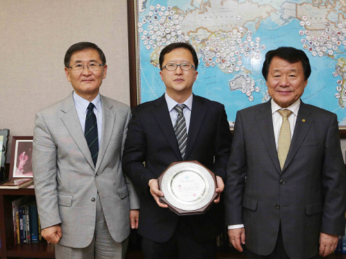 Professor Jang Wook Choi Received the Scientist of the Month Award from Daejeon City
Professor Jang Wook Choi of the Graduate School of EEWS (Energy, Environment, Water, and Sustainability), KAIST, received the “Scientist of the Month Award” from the City of Daejeon.
Mayor Hong-chul Yeom visited KAIST on May 30, 2014 and presented the award to Professor Choi.
Professor Choi has achieved research excellence over a period of time in the field of rechargeable battery, supercapacitor, and materials chemistry.
In the picture below: President Steve Kang (left), Professor Jang Wook Choi (middle), and Mayor Hong-chul Yeom (right)
2014.06.05 View 9515
Professor Jang Wook Choi Received the Scientist of the Month Award from Daejeon City
Professor Jang Wook Choi of the Graduate School of EEWS (Energy, Environment, Water, and Sustainability), KAIST, received the “Scientist of the Month Award” from the City of Daejeon.
Mayor Hong-chul Yeom visited KAIST on May 30, 2014 and presented the award to Professor Choi.
Professor Choi has achieved research excellence over a period of time in the field of rechargeable battery, supercapacitor, and materials chemistry.
In the picture below: President Steve Kang (left), Professor Jang Wook Choi (middle), and Mayor Hong-chul Yeom (right)
2014.06.05 View 9515 -
 Professor YongKeun Park Produces Undergraduate Students with International Achievements
Three undergraduate students under the supervision of Professor YongKeun Park from the Department of Physics, KAIST, have published papers in globally renowned academic journals.
The most recent publication was made by YoungJu Jo, a senior in physics. Jo’s paper entitled “Angle-resolved light scattering of individual rod-shaped bacteria based on Fourier transform light scattering” was published in the May 28th edition of Scientific Reports.
Analyzing bacteria is a very important task in the field of health and food hygiene, but using the conventional biochemical methods of analysis takes days. However, observation with Jo’s newly developed method using light scattering analyzes bacteria within a matter of seconds.
SangYeon Cho from the Department of Chemistry also published papers in Cell (2012) and Nature (2013), respectively, under the guidance of Professor Park. SangYeon Cho’s outstanding research achievements were recognized by Harvard and MIT. He was accepted with a full scholarship to Harvard-MIT Health Sciences and Technology Graduate School. He will begin his graduate studies at Harvard-MIT this September.
Last March, SeoEun Lee from the Department of Biology was the recipient of the Best Paper Award by the Optical Society of Korea. She plans to pursue a doctoral degree at the College of Physicians and Surgeons, Columbia University in New York.
Professor Park said, “Undergraduate students, who are learning a variety of subjects concurrently, are at the most creative time of their lives. KAIST has offered many opportunities to undergraduate students to partake in various research programs.”
- Picture (a) and (b): Rod-shaped bacteria’s phase image and light-scattering patterns
- Picture (c): Quantitative analysis to illustrate the extraction of information from bacteria
2014.06.03 View 16010
Professor YongKeun Park Produces Undergraduate Students with International Achievements
Three undergraduate students under the supervision of Professor YongKeun Park from the Department of Physics, KAIST, have published papers in globally renowned academic journals.
The most recent publication was made by YoungJu Jo, a senior in physics. Jo’s paper entitled “Angle-resolved light scattering of individual rod-shaped bacteria based on Fourier transform light scattering” was published in the May 28th edition of Scientific Reports.
Analyzing bacteria is a very important task in the field of health and food hygiene, but using the conventional biochemical methods of analysis takes days. However, observation with Jo’s newly developed method using light scattering analyzes bacteria within a matter of seconds.
SangYeon Cho from the Department of Chemistry also published papers in Cell (2012) and Nature (2013), respectively, under the guidance of Professor Park. SangYeon Cho’s outstanding research achievements were recognized by Harvard and MIT. He was accepted with a full scholarship to Harvard-MIT Health Sciences and Technology Graduate School. He will begin his graduate studies at Harvard-MIT this September.
Last March, SeoEun Lee from the Department of Biology was the recipient of the Best Paper Award by the Optical Society of Korea. She plans to pursue a doctoral degree at the College of Physicians and Surgeons, Columbia University in New York.
Professor Park said, “Undergraduate students, who are learning a variety of subjects concurrently, are at the most creative time of their lives. KAIST has offered many opportunities to undergraduate students to partake in various research programs.”
- Picture (a) and (b): Rod-shaped bacteria’s phase image and light-scattering patterns
- Picture (c): Quantitative analysis to illustrate the extraction of information from bacteria
2014.06.03 View 16010 -
 MOU for Intellectual Property Protection and Patent Litigation System Development
KAIST and the Patent Court of Korea signed a memorandum of understanding (MOU) to cooperate for the protection of intellectual property rights and education of patent litigation system. About 20 attendees including President Steve Kang of KAIST and Chief Justice Young-Ho Kang of the Patent Court of Korea met on May 30 at KAIST.
Through the MOU, KAIST will provide technical advice needed for the patent application process. Likewise, the Patent Court will support KAIST researchers and students by offering patent application classes and patent trial observation programs.
After the ceremony, the Patent Court hosted a class under the theme “A more realistic patent process for scientists.”
The first speaker, the Honorable Chun-Woo Son, a former judge, shared a story in which a research achievement was wasted because of scientists’ ignorance of the patent system and its procedures.
The next speaker was Dong-Yeob Kim, a patent examiner. In his lecture, titled “Proper Compensation for Inventions,” Kim emphasized the economic importance of registering patents even if the research achievements of scientists are minor.”
To further this MOU, KAIST and the Patent Court of Korea will continue to expand their cooperation into the adjacent scientific community, Daedeok Innopolis.
2014.06.03 View 8428
MOU for Intellectual Property Protection and Patent Litigation System Development
KAIST and the Patent Court of Korea signed a memorandum of understanding (MOU) to cooperate for the protection of intellectual property rights and education of patent litigation system. About 20 attendees including President Steve Kang of KAIST and Chief Justice Young-Ho Kang of the Patent Court of Korea met on May 30 at KAIST.
Through the MOU, KAIST will provide technical advice needed for the patent application process. Likewise, the Patent Court will support KAIST researchers and students by offering patent application classes and patent trial observation programs.
After the ceremony, the Patent Court hosted a class under the theme “A more realistic patent process for scientists.”
The first speaker, the Honorable Chun-Woo Son, a former judge, shared a story in which a research achievement was wasted because of scientists’ ignorance of the patent system and its procedures.
The next speaker was Dong-Yeob Kim, a patent examiner. In his lecture, titled “Proper Compensation for Inventions,” Kim emphasized the economic importance of registering patents even if the research achievements of scientists are minor.”
To further this MOU, KAIST and the Patent Court of Korea will continue to expand their cooperation into the adjacent scientific community, Daedeok Innopolis.
2014.06.03 View 8428 -
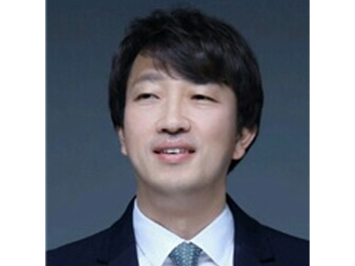
 KAIST's graduate, the first Ph.D. holder in games, is appointed professor at Michigan State University in East Lansing
Dr. Tae-Woo Park
The academic community recognizes the study in games as a field for research
Dr. Tae-Woo Park, a graduate of KAIST, has been appointed a professor at Michigan State University (MSU) in East Lansing. He will start working in August at the Department of Telecommunications, Information Studies, and Media, the College of Communications Arts, MSU.
Dr. Park received a doctoral degree in games, the first of its kind in KAIST. His research focus is game design, research, and development.
Dr. Park has strived to enhance user experience by incorporating various aspects of everyday life into games and made efforts to introduce measures limiting or preventing game addiction, a major concern among young people in South Korea. Professor Joon-Hwa Song of Computer Science at KAIST, Dr. Park's advisor, commented that "KAIST graduates have been the main actors in the development of Korea's gaming industry. Our efforts to systemize the field of games into an academic discipline have been recognized through Dr. Park's appointment."
Dr. Park said that he plans "to apply mobile device and ubiquitous technology and develop games that will not only entertain users but also help them have a better life.”
2014.05.29 View 13198
KAIST's graduate, the first Ph.D. holder in games, is appointed professor at Michigan State University in East Lansing
Dr. Tae-Woo Park
The academic community recognizes the study in games as a field for research
Dr. Tae-Woo Park, a graduate of KAIST, has been appointed a professor at Michigan State University (MSU) in East Lansing. He will start working in August at the Department of Telecommunications, Information Studies, and Media, the College of Communications Arts, MSU.
Dr. Park received a doctoral degree in games, the first of its kind in KAIST. His research focus is game design, research, and development.
Dr. Park has strived to enhance user experience by incorporating various aspects of everyday life into games and made efforts to introduce measures limiting or preventing game addiction, a major concern among young people in South Korea. Professor Joon-Hwa Song of Computer Science at KAIST, Dr. Park's advisor, commented that "KAIST graduates have been the main actors in the development of Korea's gaming industry. Our efforts to systemize the field of games into an academic discipline have been recognized through Dr. Park's appointment."
Dr. Park said that he plans "to apply mobile device and ubiquitous technology and develop games that will not only entertain users but also help them have a better life.”
2014.05.29 View 13198