Chem
-
 A Comprehensive Metabolic Map for Bio-Based Chemicals Production
A KAIST research team completed a metabolic map that charts all available strategies and pathways of chemical reactions that lead to the production of various industrial bio-based chemicals.
The team was led by Distinguished Professor Sang Yup Lee, who has produced high-quality metabolic engineering and systems engineering research for decades, and made the hallmark chemicals map after seven years of studies.
The team presented a very detailed analysis on metabolic engineering for the production of a wide range of industrial chemicals, fuels, and materials. Surveying the current trends in the bio-based production of chemicals in industrial biotechnology, the team thoroughly examined the current status of industrial chemicals produced using biological and/or chemical reactions.
This comprehensive map is expected to serve as a blueprint for the visual and intuitive inspection of biological and/or chemical reactions for the production of interest from renewable resources. The team also compiled an accompanying poster to visually present the synthetic pathways of chemicals in the context of their microbial metabolism.
As metabolic engineering has become increasing powerful in addressing limited fossil resources, climate change, and other environmental issues, the number of microbially produced chemicals using biomass as a carbon source has increased substantially. The sustainable production of industrial chemicals and materials has been explored with micro-organisms as cell factories and renewable nonfood biomass as raw materials for alternative petroleum. The engineering of these micro-organism has increasingly become more efficient and effective with the help of metabolic engineering – a practice of engineering using the metabolism of living organisms to produce a desired metabolite.
With the establishment of systems metabolic engineering – the integration of metabolic engineering with tools and strategies from systems biology, synthetic biology and evolutionary engineering – the speed at which micro-organisms are being engineered has reached an unparalleled pace.
In order to evaluate the current state at which metabolically engineered micro-organisms can produce a large portfolio of industrial chemicals, the team conducted an extensive review of the literature and mapped them out on a poster. This resulting poster, termed the bio-based chemicals map, presents synthetic pathways for industrial chemicals, which consist of biological and/or chemical reactions.
Industrial chemicals and their production routes are presented in the context of central carbon metabolic pathways as these key metabolites serve as precursors for the chemicals to be produced. The resulting biochemical map allows the detection and analysis of optimal synthetic pathways for a given industrial chemical. In addition to the poster, the authors have compiled a list of chemicals that have successfully been produced using micro-organisms and a list of the corresponding companies producing them commercially. This thorough review of the literature and the accompanying analytical summary will be an important resource for researchers interested in the production of chemicals from renewable biomass sources.
Metabolically engineered micro-organisms have already made a huge contribution toward the sustainable production of chemicals using renewable resources. Professor Lee said he wanted a detailed survey of the current state and capacity of bio-based chemicals production.
“We are so excited that this review and poster will expand further discussion on the production of important chemicals through engineered micro-organisms and also combined biological and chemical means in a more sustainable manner,” he explained.
This work was supported by the Technology Development Program to Solve Climate Changes on Systems Metabolic Engineering for Biofineries from the Ministry of Science and ICT through the National Research Foundation of Korea.
For further information, Distinguished Professor Sang Yup Lee of the Department of Chemical and Biomolecular Engineering at KAIST ( leesy@kaist.ac.kr , Tel: +82-42-350-3930)
Figure: Bio-based chemicals production through biological and chemical routes. This metabolic map describes representative chemicals that can be produced either by biological and/or chemical means. Red arrows represent chemical routes and blue arrows represent biological routes. Intermediate metabolites in the metabolism of a living organism can serve as a platform toward the production of industrially relevant chemicals. A more comprehensive map presented by the team can be found as a poster in the review.
2019.01.15 View 7736
A Comprehensive Metabolic Map for Bio-Based Chemicals Production
A KAIST research team completed a metabolic map that charts all available strategies and pathways of chemical reactions that lead to the production of various industrial bio-based chemicals.
The team was led by Distinguished Professor Sang Yup Lee, who has produced high-quality metabolic engineering and systems engineering research for decades, and made the hallmark chemicals map after seven years of studies.
The team presented a very detailed analysis on metabolic engineering for the production of a wide range of industrial chemicals, fuels, and materials. Surveying the current trends in the bio-based production of chemicals in industrial biotechnology, the team thoroughly examined the current status of industrial chemicals produced using biological and/or chemical reactions.
This comprehensive map is expected to serve as a blueprint for the visual and intuitive inspection of biological and/or chemical reactions for the production of interest from renewable resources. The team also compiled an accompanying poster to visually present the synthetic pathways of chemicals in the context of their microbial metabolism.
As metabolic engineering has become increasing powerful in addressing limited fossil resources, climate change, and other environmental issues, the number of microbially produced chemicals using biomass as a carbon source has increased substantially. The sustainable production of industrial chemicals and materials has been explored with micro-organisms as cell factories and renewable nonfood biomass as raw materials for alternative petroleum. The engineering of these micro-organism has increasingly become more efficient and effective with the help of metabolic engineering – a practice of engineering using the metabolism of living organisms to produce a desired metabolite.
With the establishment of systems metabolic engineering – the integration of metabolic engineering with tools and strategies from systems biology, synthetic biology and evolutionary engineering – the speed at which micro-organisms are being engineered has reached an unparalleled pace.
In order to evaluate the current state at which metabolically engineered micro-organisms can produce a large portfolio of industrial chemicals, the team conducted an extensive review of the literature and mapped them out on a poster. This resulting poster, termed the bio-based chemicals map, presents synthetic pathways for industrial chemicals, which consist of biological and/or chemical reactions.
Industrial chemicals and their production routes are presented in the context of central carbon metabolic pathways as these key metabolites serve as precursors for the chemicals to be produced. The resulting biochemical map allows the detection and analysis of optimal synthetic pathways for a given industrial chemical. In addition to the poster, the authors have compiled a list of chemicals that have successfully been produced using micro-organisms and a list of the corresponding companies producing them commercially. This thorough review of the literature and the accompanying analytical summary will be an important resource for researchers interested in the production of chemicals from renewable biomass sources.
Metabolically engineered micro-organisms have already made a huge contribution toward the sustainable production of chemicals using renewable resources. Professor Lee said he wanted a detailed survey of the current state and capacity of bio-based chemicals production.
“We are so excited that this review and poster will expand further discussion on the production of important chemicals through engineered micro-organisms and also combined biological and chemical means in a more sustainable manner,” he explained.
This work was supported by the Technology Development Program to Solve Climate Changes on Systems Metabolic Engineering for Biofineries from the Ministry of Science and ICT through the National Research Foundation of Korea.
For further information, Distinguished Professor Sang Yup Lee of the Department of Chemical and Biomolecular Engineering at KAIST ( leesy@kaist.ac.kr , Tel: +82-42-350-3930)
Figure: Bio-based chemicals production through biological and chemical routes. This metabolic map describes representative chemicals that can be produced either by biological and/or chemical means. Red arrows represent chemical routes and blue arrows represent biological routes. Intermediate metabolites in the metabolism of a living organism can serve as a platform toward the production of industrially relevant chemicals. A more comprehensive map presented by the team can be found as a poster in the review.
2019.01.15 View 7736 -
 Fabrication of Shape-conformable Batteries with 3D-Printing
(from left: Dr. Bok Yeop Ahn, Dr. Chanhoon Kim, Professor Il-Doo Kim and Professor Jennifer A. Lewis)
Flexible, wireless electronic devices are rapidly emerging and have reached the level of commercialization; nevertheless, most of battery shapes are limited to either spherical and/or rectangular structures, which results in inefficient space use. Professor Il-Doo Kim’s team from the Department of Materials Science at KAIST has successfully developed technology to significantly enhance the variability of battery design through collaboration research with Professor Jennifer A. Lewis and her team from the School of Engineering and Applied Sciences at Harvard University.
Most of the battery shapes today are optimized for coin cell and/or pouch cells. Since the battery as an energy storage device occupies most of the space in microelectronic devices with different designs, new technology to freely change the shape of the battery is required.
The KAIST-Harvard research collaboration team has successfully manufactured various kinds of battery shapes, such as ring-type, H, and U shape, using 3D printing technology. And through the research collaboration with Dr. Youngmin Choi at the Korea Research Institute of Chemical Technology (KRICT), 3D-printed batteries were applied to small-scale wearable electronic devices (wearable light sensor rings).
The research group has adopted environmentally friendly aqueous Zn-ion batteries to make customized battery packs. This system, which uses Zn2+ instead of Li+ as charge carriers, is much safer compared with the conventional lithium rechargeable batteries that use highly inflammable organic electrolytes. Moreover, the processing conditions of lithium-ion batteries are very complicated because organic solvents can ignite upon exposure to moisture and oxygen.
As the aqueous Zn-ion batteries adopted by the research team are stable upon contact with atmospheric moisture and oxygen, they can be fabricated in the ambient air condition, and have advantages in packaging since packaged plastic does not dissolve in water even when plastic packaging is applied using a 3D printer.
To fabricate a stable cathode that can be modulated in various forms and allows high charge-discharge, the research team fabricated a carbon fiber current collector using electrospinning process and uniformly coated electrochemically active polyaniline conductive polymer on the surface of carbon fiber for a current collector-active layer integrated cathode. The cathode, based on conductive polyaniline consisting of a 3D structure, exhibits very fast charging speeds (50% of the charge in two minutes) and can be fabricated without the detachment of active cathode materials, so various battery forms with high mechanical stability can be manufactured.
Prof. Kim said, “Zn-ion batteries employing aqueous electrolytes have the advantage of fabrication under ambient conditions, so it is easy to fabricate the customized battery packs using 3D printing.”
“3D-printed batteries can be easily applied for niche applications such as wearable, personalized, miniaturized micro-robots, and implantable medical devices or microelectronic storage devices with unique designs,” added Professor Lewis.
With Dr. Chanhoon Kim in the Department of Materials Science and Engineering at KAIST and Dr. Bok Yeop Ahn School of Engineering and Applied Sciences at Harvard University participating as equally contributing first authors, this work was published in the December issue of ACS Nano.
This work was financially supported by the Global Research Laboratory (NRF-2015K1A1A2029679) and Wearable Platform Materials Technology Center (2016R1A5A1009926).
Figure 1.Fabrication of shape-conformable batteries based on 3D-printing technology and the application of polyaniline carbon nanofiber cathodes and wearable electronic devices
Figure 2.Fabricated shape-conformable batteries based on a 3D-printing method
Meanwhile, Professor Il-Doo Kim was recently appointed as an Associate Editor of ACS Nano, a highly renowned journal in the field of nanoscience.
Professor Kim said, “It is my great honor to be an Associate Editor of the highly renowned journal ACS Nano, which has an impact factor reaching 13.709 with 134,596 citations as of 2017. Through the editorial activities in the fields of energy, I will dedicate myself to improving the prominence of KAIST and expanding the scope of Korea’s science and technology. I will also contribute to carrying out more international collaborations with world-leading research groups.”
(Associate Editor of ACS Nano Professor Il-Doo Kim)
2018.12.20 View 11253
Fabrication of Shape-conformable Batteries with 3D-Printing
(from left: Dr. Bok Yeop Ahn, Dr. Chanhoon Kim, Professor Il-Doo Kim and Professor Jennifer A. Lewis)
Flexible, wireless electronic devices are rapidly emerging and have reached the level of commercialization; nevertheless, most of battery shapes are limited to either spherical and/or rectangular structures, which results in inefficient space use. Professor Il-Doo Kim’s team from the Department of Materials Science at KAIST has successfully developed technology to significantly enhance the variability of battery design through collaboration research with Professor Jennifer A. Lewis and her team from the School of Engineering and Applied Sciences at Harvard University.
Most of the battery shapes today are optimized for coin cell and/or pouch cells. Since the battery as an energy storage device occupies most of the space in microelectronic devices with different designs, new technology to freely change the shape of the battery is required.
The KAIST-Harvard research collaboration team has successfully manufactured various kinds of battery shapes, such as ring-type, H, and U shape, using 3D printing technology. And through the research collaboration with Dr. Youngmin Choi at the Korea Research Institute of Chemical Technology (KRICT), 3D-printed batteries were applied to small-scale wearable electronic devices (wearable light sensor rings).
The research group has adopted environmentally friendly aqueous Zn-ion batteries to make customized battery packs. This system, which uses Zn2+ instead of Li+ as charge carriers, is much safer compared with the conventional lithium rechargeable batteries that use highly inflammable organic electrolytes. Moreover, the processing conditions of lithium-ion batteries are very complicated because organic solvents can ignite upon exposure to moisture and oxygen.
As the aqueous Zn-ion batteries adopted by the research team are stable upon contact with atmospheric moisture and oxygen, they can be fabricated in the ambient air condition, and have advantages in packaging since packaged plastic does not dissolve in water even when plastic packaging is applied using a 3D printer.
To fabricate a stable cathode that can be modulated in various forms and allows high charge-discharge, the research team fabricated a carbon fiber current collector using electrospinning process and uniformly coated electrochemically active polyaniline conductive polymer on the surface of carbon fiber for a current collector-active layer integrated cathode. The cathode, based on conductive polyaniline consisting of a 3D structure, exhibits very fast charging speeds (50% of the charge in two minutes) and can be fabricated without the detachment of active cathode materials, so various battery forms with high mechanical stability can be manufactured.
Prof. Kim said, “Zn-ion batteries employing aqueous electrolytes have the advantage of fabrication under ambient conditions, so it is easy to fabricate the customized battery packs using 3D printing.”
“3D-printed batteries can be easily applied for niche applications such as wearable, personalized, miniaturized micro-robots, and implantable medical devices or microelectronic storage devices with unique designs,” added Professor Lewis.
With Dr. Chanhoon Kim in the Department of Materials Science and Engineering at KAIST and Dr. Bok Yeop Ahn School of Engineering and Applied Sciences at Harvard University participating as equally contributing first authors, this work was published in the December issue of ACS Nano.
This work was financially supported by the Global Research Laboratory (NRF-2015K1A1A2029679) and Wearable Platform Materials Technology Center (2016R1A5A1009926).
Figure 1.Fabrication of shape-conformable batteries based on 3D-printing technology and the application of polyaniline carbon nanofiber cathodes and wearable electronic devices
Figure 2.Fabricated shape-conformable batteries based on a 3D-printing method
Meanwhile, Professor Il-Doo Kim was recently appointed as an Associate Editor of ACS Nano, a highly renowned journal in the field of nanoscience.
Professor Kim said, “It is my great honor to be an Associate Editor of the highly renowned journal ACS Nano, which has an impact factor reaching 13.709 with 134,596 citations as of 2017. Through the editorial activities in the fields of energy, I will dedicate myself to improving the prominence of KAIST and expanding the scope of Korea’s science and technology. I will also contribute to carrying out more international collaborations with world-leading research groups.”
(Associate Editor of ACS Nano Professor Il-Doo Kim)
2018.12.20 View 11253 -
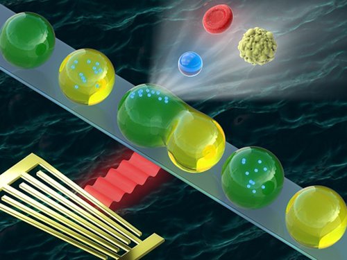 Washing and Enrichment of Micro-Particles Encapsulated in Droplets
Researchers developed microfluidic technology for the washing and enrichment of in-droplet micro-particles. They presented the technology using a microfluidic chip based on surface acoustic wave (SAW)-driven acoustic radiation force (ARF).
The team demonstrated the first instance of acoustic in-droplet micro-particle washing with a particle recovery rate of approximately 90 percent. They further extended the applicability of the proposed method to in-droplet particle enrichment with the unprecedented abilities to increase the in-droplet particle quantity and exchange the droplet dispersed phase.
This proposed method enabled on-chip, label-free, continuous, and selective in-droplet micro-particle manipulation. The team demonstrated the first instance of in-droplet micro-particle washing between two types of alternating droplets in a simple microchannel, proving that the method can increase the particle quantity, which has not been achieved by previously reported methods.
The study aimed to develop an in-droplet micro-particle washing and enrichment method based on SAW-driven ARF. When a droplet containing particles is exposed to an acoustic field, both the droplet and suspended particles experience ARF arising from inhomogeneous wave scattering at the liquid-liquid and liquid-solid interfaces. Unlike previous in-droplet particle manipulation methods, this method allows simultaneous and precise control over the droplets and suspended particles. Moreover, the proposed acoustic method does not require labelled particles, such as magnetic particles, and employs a simple microchannel geometry.
Microfluidic sample washing has emerged as an alternative to centrifugation because the limitations of centrifugation-based washing methods can be addressed using continuous washing processes. It also has considerable potential and importance in a variety of applications such as single-cell/particle assays, high-throughput screening of rare samples, and cell culture medium exchange.
Compared to continuous flow-based microfluidic methods, droplet-based microfluidic sample washing has been rarely explored due to technological difficulties. On-chip, in-droplet sample washing requires sample transfer across the droplet interface composed of two immiscible fluids. This process involves simultaneous and precise control over the encapsulated sample and droplet interface during the medium exchange of the in-droplet sample.
Sample encapsulation within individual microscale droplets offers isolated microenvironments for the samples. Experimental uncertainties due to cross-contamination and Taylor dispersion between multiple reagents can be reduced in droplet-based microfluidics.
This is the first research achievement made by the Acousto-Microfluidics Research Center for Next-Generation Healthcare, the cross-generation collaborative lab KAIST opened in May. This novel approach pairs senior and junior faculty members for sustaining the research legacy even after the senior researcher retires. The research center, which paired Chair Professor Hyung Jin Sung and Professors Hyoungsoo Kim and Yeunwoo Cho, made a breakthrough in microfluidics along with PhD candidate Jinsoo Park. The study was featured as the cover of Lab on a Chip published by Royal Society of Chemistry.
Jinsoo Park, first author of the study, believes this technology will may serve as an in-droplet sample preparation platform with in-line integration of other droplet microfluidic components. Chair Professor Sung said, “The proposed acoustic method will offer new perspectives on sample washing and enrichment by performing the operation in microscale droplets.”
Figure 1. (a) A microfluidic device for in-droplet micro-particle washing and enrichment; (b) alternatingly produced droplets of two kinds at a double T-junction; (c) a droplet and encapsulated micro-particles exposed to surface acoustic wave-driven acoustic radiation force; (d-h) sequential processes of in-droplet micro-particle washing and enrichment operation.
2018.10.19 View 8258
Washing and Enrichment of Micro-Particles Encapsulated in Droplets
Researchers developed microfluidic technology for the washing and enrichment of in-droplet micro-particles. They presented the technology using a microfluidic chip based on surface acoustic wave (SAW)-driven acoustic radiation force (ARF).
The team demonstrated the first instance of acoustic in-droplet micro-particle washing with a particle recovery rate of approximately 90 percent. They further extended the applicability of the proposed method to in-droplet particle enrichment with the unprecedented abilities to increase the in-droplet particle quantity and exchange the droplet dispersed phase.
This proposed method enabled on-chip, label-free, continuous, and selective in-droplet micro-particle manipulation. The team demonstrated the first instance of in-droplet micro-particle washing between two types of alternating droplets in a simple microchannel, proving that the method can increase the particle quantity, which has not been achieved by previously reported methods.
The study aimed to develop an in-droplet micro-particle washing and enrichment method based on SAW-driven ARF. When a droplet containing particles is exposed to an acoustic field, both the droplet and suspended particles experience ARF arising from inhomogeneous wave scattering at the liquid-liquid and liquid-solid interfaces. Unlike previous in-droplet particle manipulation methods, this method allows simultaneous and precise control over the droplets and suspended particles. Moreover, the proposed acoustic method does not require labelled particles, such as magnetic particles, and employs a simple microchannel geometry.
Microfluidic sample washing has emerged as an alternative to centrifugation because the limitations of centrifugation-based washing methods can be addressed using continuous washing processes. It also has considerable potential and importance in a variety of applications such as single-cell/particle assays, high-throughput screening of rare samples, and cell culture medium exchange.
Compared to continuous flow-based microfluidic methods, droplet-based microfluidic sample washing has been rarely explored due to technological difficulties. On-chip, in-droplet sample washing requires sample transfer across the droplet interface composed of two immiscible fluids. This process involves simultaneous and precise control over the encapsulated sample and droplet interface during the medium exchange of the in-droplet sample.
Sample encapsulation within individual microscale droplets offers isolated microenvironments for the samples. Experimental uncertainties due to cross-contamination and Taylor dispersion between multiple reagents can be reduced in droplet-based microfluidics.
This is the first research achievement made by the Acousto-Microfluidics Research Center for Next-Generation Healthcare, the cross-generation collaborative lab KAIST opened in May. This novel approach pairs senior and junior faculty members for sustaining the research legacy even after the senior researcher retires. The research center, which paired Chair Professor Hyung Jin Sung and Professors Hyoungsoo Kim and Yeunwoo Cho, made a breakthrough in microfluidics along with PhD candidate Jinsoo Park. The study was featured as the cover of Lab on a Chip published by Royal Society of Chemistry.
Jinsoo Park, first author of the study, believes this technology will may serve as an in-droplet sample preparation platform with in-line integration of other droplet microfluidic components. Chair Professor Sung said, “The proposed acoustic method will offer new perspectives on sample washing and enrichment by performing the operation in microscale droplets.”
Figure 1. (a) A microfluidic device for in-droplet micro-particle washing and enrichment; (b) alternatingly produced droplets of two kinds at a double T-junction; (c) a droplet and encapsulated micro-particles exposed to surface acoustic wave-driven acoustic radiation force; (d-h) sequential processes of in-droplet micro-particle washing and enrichment operation.
2018.10.19 View 8258 -
 The 1st Korea Toray Science and Technology Awardee, Prof. Sukbok Chang
(Distinguished Professor Sukbok Chang from the Department of Chemistry)
The Korea Toray Science Foundation (KTSF) awarded the first Korea Toray Science Technology Award in basic science to Distinguished Professor Sukbok Chang from the Department of Chemistry on September 19.
KTSF was established in January 2018, and its award goes to researchers who have significantly contributed to the development of chemistry and materials research with funds to support research projects.
Distinguished Professor Chang has devoted himself in organocatalysis research; in particular, his work on catalysts for effective lactam formation, which was an intricate problem, received great attention.
The award ceremony will take place in The Federation of Korean Industries Hall on October 31. KTFS board members, judges, and the CEO of Toray Industries Akihiro Nikkaku will attend the ceremony. Also, Dr. Ryoji Noyori, the Nobel Laureate in Chemistry, will give a talk on the role of chemistry and creative challenges as a researcher.
2018.10.04 View 9553
The 1st Korea Toray Science and Technology Awardee, Prof. Sukbok Chang
(Distinguished Professor Sukbok Chang from the Department of Chemistry)
The Korea Toray Science Foundation (KTSF) awarded the first Korea Toray Science Technology Award in basic science to Distinguished Professor Sukbok Chang from the Department of Chemistry on September 19.
KTSF was established in January 2018, and its award goes to researchers who have significantly contributed to the development of chemistry and materials research with funds to support research projects.
Distinguished Professor Chang has devoted himself in organocatalysis research; in particular, his work on catalysts for effective lactam formation, which was an intricate problem, received great attention.
The award ceremony will take place in The Federation of Korean Industries Hall on October 31. KTFS board members, judges, and the CEO of Toray Industries Akihiro Nikkaku will attend the ceremony. Also, Dr. Ryoji Noyori, the Nobel Laureate in Chemistry, will give a talk on the role of chemistry and creative challenges as a researcher.
2018.10.04 View 9553 -
 Spray Coated Tactile Sensor on a 3-D Surface for Robotic Skin
Robots will be able to conduct a wide variety of tasks as well as humans if they can be given tactile sensing capabilities.
A KAIST research team has reported a stretchable pressure insensitive strain sensor by using an all solution-based process. The solution-based process is easily scalable to accommodate for large areas and can be coated as a thin-film on 3-dimensional irregularly shaped objects via spray coating. These conditions make their processing technique unique and highly suitable for robotic electronic skin or wearable electronic applications.
The making of electronic skin to mimic the tactile sensing properties of human skin is an active area of research for various applications such as wearable electronics, robotics, and prosthetics. One of the major challenges in electronic skin research is differentiating various external stimuli, particularly between strain and pressure. Another issue is uniformly depositing electrical skin on 3-dimensional irregularly shaped objects.
To overcome these issues, the research team led by Professor Steve Park from the Department of Materials Science and Engineering and Professor Jung Kim from the Department of Mechanical Engineering developed electronic skin that can be uniformly coated on 3-dimensional surfaces and distinguish mechanical stimuli. The new electronic skin can also distinguish mechanical stimuli analogous to human skin. The structure of the electronic skin was designed to respond differently under applied pressure and strain. Under applied strain, conducting pathways undergo significant conformational changes, considerably changing the resistance. On the other hand, under applied pressure, negligible conformational change in the conducting pathway occurs; e-skin is therefore non-responsive to pressure. The research team is currently working on strain insensitive pressure sensors to use with the developed strain sensors.
The research team also spatially mapped the local strain without the use of patterned electrode arrays utilizing electrical impedance tomography (EIT). By using EIT, it is possible to minimize the number of electrodes, increase durability, and enable facile fabrication onto 3-dimensional surfaces.
Professor Park said, “Our electronic skin can be mass produced at a low cost and can easily be coated onto complex 3-dimensional surfaces. It is a key technology that can bring us closer to the commercialization of electronic skin for various applications in the near future.”
The result of this work entitled “Pressure Insensitive Strain Sensor with Facile Solution-based Process for Tactile Sensing Applications” was published in the August issue of ACS Nano as a cover article.
(Figure: Detecting mechanical stimuli using electrical impedance tomography.)
2018.09.21 View 8892
Spray Coated Tactile Sensor on a 3-D Surface for Robotic Skin
Robots will be able to conduct a wide variety of tasks as well as humans if they can be given tactile sensing capabilities.
A KAIST research team has reported a stretchable pressure insensitive strain sensor by using an all solution-based process. The solution-based process is easily scalable to accommodate for large areas and can be coated as a thin-film on 3-dimensional irregularly shaped objects via spray coating. These conditions make their processing technique unique and highly suitable for robotic electronic skin or wearable electronic applications.
The making of electronic skin to mimic the tactile sensing properties of human skin is an active area of research for various applications such as wearable electronics, robotics, and prosthetics. One of the major challenges in electronic skin research is differentiating various external stimuli, particularly between strain and pressure. Another issue is uniformly depositing electrical skin on 3-dimensional irregularly shaped objects.
To overcome these issues, the research team led by Professor Steve Park from the Department of Materials Science and Engineering and Professor Jung Kim from the Department of Mechanical Engineering developed electronic skin that can be uniformly coated on 3-dimensional surfaces and distinguish mechanical stimuli. The new electronic skin can also distinguish mechanical stimuli analogous to human skin. The structure of the electronic skin was designed to respond differently under applied pressure and strain. Under applied strain, conducting pathways undergo significant conformational changes, considerably changing the resistance. On the other hand, under applied pressure, negligible conformational change in the conducting pathway occurs; e-skin is therefore non-responsive to pressure. The research team is currently working on strain insensitive pressure sensors to use with the developed strain sensors.
The research team also spatially mapped the local strain without the use of patterned electrode arrays utilizing electrical impedance tomography (EIT). By using EIT, it is possible to minimize the number of electrodes, increase durability, and enable facile fabrication onto 3-dimensional surfaces.
Professor Park said, “Our electronic skin can be mass produced at a low cost and can easily be coated onto complex 3-dimensional surfaces. It is a key technology that can bring us closer to the commercialization of electronic skin for various applications in the near future.”
The result of this work entitled “Pressure Insensitive Strain Sensor with Facile Solution-based Process for Tactile Sensing Applications” was published in the August issue of ACS Nano as a cover article.
(Figure: Detecting mechanical stimuli using electrical impedance tomography.)
2018.09.21 View 8892 -
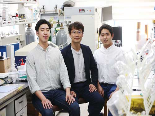 KAIST Develops VRFB with Longer Durability
(from left: PhD candidate Soohyun Kim, Professor Hee-Tak Kim and PhD candidate Junghoon Choi)
There has been growing demand for large-scale storage for energy produced from renewable energy sources in an efficient and stable way. To meet this demand, a KAIST research team developed a new vanadium redox-flow battery (VRFB) with 15 times greater capacity retention and five times longer durability. This VRFB battery can be an excellent candidate for a large-scale rechargeable battery with no risk of explosion.
The VRFB has received much attention for its high efficiency and reliability with the absence of cross-contamination. However, it has the limitation of having insufficient charge and discharge efficiency and a low capacity retention rate because its perfluorinated membrane is very permeable to any active materials. To minimize energy loss, it needs a membrane that has low vanadium ion permeability and high ion conductivity. Hence, there was an attempt to incorporate a hydrocarbon membrane that has low cost and high ion selectivity but it turned out that the VO₂+ caused chemical degradation, which led to shortening the battery life drastically.
To develop a membrane with pore sizes smaller than the hydrated size of vanadium ions yet larger than that of the protons, a research team co-led by Professor Hee-Tae Jung and Professor Hee-Tak Kim from the Department of Chemical and Biomolecular Engineering implemented a graphene-oxide framework (GOF) membrane by cross-linking graphene oxide nanosheets. They believed that GOF, having strong ion selectivity, would be a good candidate for the membrane component for the VRFB. The interlayer spacing between the GO sheets limited moisture expansion and provided selective ion permeation.
The GOF membrane increased the capacity retention of the VRFB, which showed a 15 times higher rate than that of perfluorinated membranes. Its cycling stability was also enhanced up to five times, compared to conventional hydrocarbon membranes.
These pore-sized-tuned graphene oxide frameworks will allow pore-sized tuning of membranes and will be applicable to electrochemical systems that utilize ions of various sizes, such as rechargeable batteries and sensors.
Professor Kim said, “Developing a membrane that prevents the mixing of positive and negative active materials has been a chronic issue in the field of redox-flow batteries. Through this research, we showed that nanotechnology can prevent this crossover issue and membrane degradation. I believe that this technology can be applied to various rechargeable batteries requiring large-scale storage.”
This research was published in Nano Letters on May 3.
Figure 1. Electrochemical performances of the VRFBs with Nafion 115, SPAES (sulfonated poly), and GOF/SPAES: discharge capacity
Figure 2. Schematic of the selective ion transfer of hydrated vanadium ions and protons in the GOF membrane and the molecular structure of the GOF membrane, showing that the GO nanosheets are cross-linked with EDA (ethylenediamine)
2018.09.20 View 7802
KAIST Develops VRFB with Longer Durability
(from left: PhD candidate Soohyun Kim, Professor Hee-Tak Kim and PhD candidate Junghoon Choi)
There has been growing demand for large-scale storage for energy produced from renewable energy sources in an efficient and stable way. To meet this demand, a KAIST research team developed a new vanadium redox-flow battery (VRFB) with 15 times greater capacity retention and five times longer durability. This VRFB battery can be an excellent candidate for a large-scale rechargeable battery with no risk of explosion.
The VRFB has received much attention for its high efficiency and reliability with the absence of cross-contamination. However, it has the limitation of having insufficient charge and discharge efficiency and a low capacity retention rate because its perfluorinated membrane is very permeable to any active materials. To minimize energy loss, it needs a membrane that has low vanadium ion permeability and high ion conductivity. Hence, there was an attempt to incorporate a hydrocarbon membrane that has low cost and high ion selectivity but it turned out that the VO₂+ caused chemical degradation, which led to shortening the battery life drastically.
To develop a membrane with pore sizes smaller than the hydrated size of vanadium ions yet larger than that of the protons, a research team co-led by Professor Hee-Tae Jung and Professor Hee-Tak Kim from the Department of Chemical and Biomolecular Engineering implemented a graphene-oxide framework (GOF) membrane by cross-linking graphene oxide nanosheets. They believed that GOF, having strong ion selectivity, would be a good candidate for the membrane component for the VRFB. The interlayer spacing between the GO sheets limited moisture expansion and provided selective ion permeation.
The GOF membrane increased the capacity retention of the VRFB, which showed a 15 times higher rate than that of perfluorinated membranes. Its cycling stability was also enhanced up to five times, compared to conventional hydrocarbon membranes.
These pore-sized-tuned graphene oxide frameworks will allow pore-sized tuning of membranes and will be applicable to electrochemical systems that utilize ions of various sizes, such as rechargeable batteries and sensors.
Professor Kim said, “Developing a membrane that prevents the mixing of positive and negative active materials has been a chronic issue in the field of redox-flow batteries. Through this research, we showed that nanotechnology can prevent this crossover issue and membrane degradation. I believe that this technology can be applied to various rechargeable batteries requiring large-scale storage.”
This research was published in Nano Letters on May 3.
Figure 1. Electrochemical performances of the VRFBs with Nafion 115, SPAES (sulfonated poly), and GOF/SPAES: discharge capacity
Figure 2. Schematic of the selective ion transfer of hydrated vanadium ions and protons in the GOF membrane and the molecular structure of the GOF membrane, showing that the GO nanosheets are cross-linked with EDA (ethylenediamine)
2018.09.20 View 7802 -
 Transfering Nanowires onto a Flexible Substrate
(from left: PhD Min-Ho Seo and Professor Jun-Bo Yoon)
Boasting excellent physical and chemical properties, nanowires (NWs) are suitable for fabricating flexible electronics; therefore, technology to transfer well-aligned wires plays a crucial role in enhancing performance of the devices. A KAIST research team succeeded in developing NW-transfer technology that is expected to enhance the existing chemical reaction-based NW fabrication technology that has this far showed low performance in applicability and productivity.
NWs, one of the most well-known nanomaterials, have the structural advantage of being small and lightweight. Hence, NW-transfer technology has drawn attention because it can fabricate high-performance, flexible nanodevices with high simplicity and throughput.
A conventional nanowire-fabrication method generally has an irregularity issue since it mixes chemically synthesized nanowires in a solution and randomly distributes the NWs onto flexible substrates. Hence, numerous nanofabrication processes have emerged, and one of them is master-mold-based, which enables the fabrication of highly ordered NW arrays embedded onto substrates in a simple and cost-effective manner, but its employment is limited to only some materials because of its chemistry-based NW-transfer mechanism, which is complex and time consuming. For the successful transfer, it requires that adequate chemicals controlling the chemical interfacial adhesion between the master mold, NWs, and flexible substrate be present.
Here, Professor Jun-Bo Yoon and his team from the School of Electrical Engineering introduced a material-independent mechanical-interlocking-based nanowire-transfer (MINT) method to fabricate ultralong and fully aligned NWs on a large flexible substrate in a highly robust manner.
This method involves sequentially forming a nanosacrificial layer and NWs on a nanograting substrate that becomes the master mold for the transfer, then weakening the structure of the nanosacrificial layer through a dry etching process. The nanosacrificial layer very weakly holds the nanowires on the master mold. Therefore, when using a flexible substrate material, the nanowires are very easily transferred from the master mold to the substrate, just like a piece of tape lifting dust off a carpet.
This technology uses common physical vapor deposition and does not rely on NW materials, making it easy to fabricate NWs onto the flexible substrates.
Using this technology, the team was able to fabricate a variety of metal and metal-oxide NWs, including gold, platinum, and copper – all perfectly aligned on a flexible substrate. They also confirmed that it can be applied to creating stable and applicable devices in everyday life by successfully applying it to flexible heaters and gas sensors.
PhD Min-Ho Seo who led this research said, “We have successfully aligned various metals and semiconductor NWs with excellent physical properties onto flexible substrates and applied them to fabricated devices. As a platform-technology, it will contribute to developing high-performing and stable electronic devices.”
This research was published in ACS Nano on May 24.
Figure 1. Photograph of the fabricated wafer-scale fully aligned and ultralong Au nanowire array on a flexible substrate
2018.09.17 View 6601
Transfering Nanowires onto a Flexible Substrate
(from left: PhD Min-Ho Seo and Professor Jun-Bo Yoon)
Boasting excellent physical and chemical properties, nanowires (NWs) are suitable for fabricating flexible electronics; therefore, technology to transfer well-aligned wires plays a crucial role in enhancing performance of the devices. A KAIST research team succeeded in developing NW-transfer technology that is expected to enhance the existing chemical reaction-based NW fabrication technology that has this far showed low performance in applicability and productivity.
NWs, one of the most well-known nanomaterials, have the structural advantage of being small and lightweight. Hence, NW-transfer technology has drawn attention because it can fabricate high-performance, flexible nanodevices with high simplicity and throughput.
A conventional nanowire-fabrication method generally has an irregularity issue since it mixes chemically synthesized nanowires in a solution and randomly distributes the NWs onto flexible substrates. Hence, numerous nanofabrication processes have emerged, and one of them is master-mold-based, which enables the fabrication of highly ordered NW arrays embedded onto substrates in a simple and cost-effective manner, but its employment is limited to only some materials because of its chemistry-based NW-transfer mechanism, which is complex and time consuming. For the successful transfer, it requires that adequate chemicals controlling the chemical interfacial adhesion between the master mold, NWs, and flexible substrate be present.
Here, Professor Jun-Bo Yoon and his team from the School of Electrical Engineering introduced a material-independent mechanical-interlocking-based nanowire-transfer (MINT) method to fabricate ultralong and fully aligned NWs on a large flexible substrate in a highly robust manner.
This method involves sequentially forming a nanosacrificial layer and NWs on a nanograting substrate that becomes the master mold for the transfer, then weakening the structure of the nanosacrificial layer through a dry etching process. The nanosacrificial layer very weakly holds the nanowires on the master mold. Therefore, when using a flexible substrate material, the nanowires are very easily transferred from the master mold to the substrate, just like a piece of tape lifting dust off a carpet.
This technology uses common physical vapor deposition and does not rely on NW materials, making it easy to fabricate NWs onto the flexible substrates.
Using this technology, the team was able to fabricate a variety of metal and metal-oxide NWs, including gold, platinum, and copper – all perfectly aligned on a flexible substrate. They also confirmed that it can be applied to creating stable and applicable devices in everyday life by successfully applying it to flexible heaters and gas sensors.
PhD Min-Ho Seo who led this research said, “We have successfully aligned various metals and semiconductor NWs with excellent physical properties onto flexible substrates and applied them to fabricated devices. As a platform-technology, it will contribute to developing high-performing and stable electronic devices.”
This research was published in ACS Nano on May 24.
Figure 1. Photograph of the fabricated wafer-scale fully aligned and ultralong Au nanowire array on a flexible substrate
2018.09.17 View 6601 -
 Rh Ensemble Catalyst for Effective Automobile Exhaust Treatment
(from left: Professor Hyunjoo Lee and PhD candidate Hojin Jeong)
A KAIST research team has developed a fully dispersed Rh ensemble catalyst (ENS) that shows better performance than commercial diesel oxidation catalyst (DOC). This newly developed ENSs could improve low-temperature automobile exhaust treatment.
Precious metals have been used for various heterogeneous reactions, but it is crucial to maximize efficiency of catalysts due to their high cost. Single-atom catalysts (SACs) have received much attention because it is possible for all of the metal atoms to be used for reactions, yet they do not show catalytic activity for reactions that require ensemble sites.
Meanwhile, hydrocarbons, such as propylene (C3H6) and propane (C3H8) are typical automobile exhaust gas pollutants and must be converted to carbon dioxide (CO2) and water (H2O) before they are released as exhaust. Since the hydrocarbon oxidation reaction proceeds only during carbon-carbon (C-C) or carbon-hydrogen (C-H) bond cleavage, it is essential to secure the metal ensemble site for the catalytic reaction. Therefore, precious metal catalysts with high dispersion and ensemble sites are greatly needed.
To solve this issue, Professor Hyunjoo Lee from the Department of Chemical and Biomolecular Engineering and Professor Jeong Woo Han from POSTECH developed an Rh ensemble catalyst with 100% dispersion, and applied it to automobile after-treatment. Having a 100% dispersion means that every metal atom is used for the reaction since it is exposed on the surface.
SACs also have 100% dispersion, but the difference is that ENSs have the unique advantage of having an ensemble site with two or more atoms.
As a result of the experiment, the ENSs showed excellent catalytic performance in CO, NO, propylene, and propane oxidation at low temperatures. This complements the disadvantage of nanoparticle catalyst (NPs) that perform catalysis poorly at low temperatures due to low metal dispersion, or SACs without hydrocarbon oxidation.
In particular, the ENSs have superior low-temperature activity even better than commercial DOC, hence they are expected to be applied to automobile exhaust treatment.
Professor Lee said, “I believe that the ENSs have given academic contribution for proposing a new concept of metal catalysts, differentiating from conventional SACs and NPs. At the same time, they are of great value in the industry of exhaust treatment catalysts.”
This research, led by PhD candidate Hojin Jeong, was published in the Journal of the American Chemical Society on July 5.
Figure 1. Concept of Rh ensemble catalyst for automobile exhaust treatment
Figure 2. Structure and performance comparison of single-atom catalyst and ensemble catalyst
Figure 3. Energy-dispersive X-ray spectroscopy (EDS) mapping images for SAC, ENS, and NP, respectively (green, Eh; red, Ce)
2018.08.29 View 7678
Rh Ensemble Catalyst for Effective Automobile Exhaust Treatment
(from left: Professor Hyunjoo Lee and PhD candidate Hojin Jeong)
A KAIST research team has developed a fully dispersed Rh ensemble catalyst (ENS) that shows better performance than commercial diesel oxidation catalyst (DOC). This newly developed ENSs could improve low-temperature automobile exhaust treatment.
Precious metals have been used for various heterogeneous reactions, but it is crucial to maximize efficiency of catalysts due to their high cost. Single-atom catalysts (SACs) have received much attention because it is possible for all of the metal atoms to be used for reactions, yet they do not show catalytic activity for reactions that require ensemble sites.
Meanwhile, hydrocarbons, such as propylene (C3H6) and propane (C3H8) are typical automobile exhaust gas pollutants and must be converted to carbon dioxide (CO2) and water (H2O) before they are released as exhaust. Since the hydrocarbon oxidation reaction proceeds only during carbon-carbon (C-C) or carbon-hydrogen (C-H) bond cleavage, it is essential to secure the metal ensemble site for the catalytic reaction. Therefore, precious metal catalysts with high dispersion and ensemble sites are greatly needed.
To solve this issue, Professor Hyunjoo Lee from the Department of Chemical and Biomolecular Engineering and Professor Jeong Woo Han from POSTECH developed an Rh ensemble catalyst with 100% dispersion, and applied it to automobile after-treatment. Having a 100% dispersion means that every metal atom is used for the reaction since it is exposed on the surface.
SACs also have 100% dispersion, but the difference is that ENSs have the unique advantage of having an ensemble site with two or more atoms.
As a result of the experiment, the ENSs showed excellent catalytic performance in CO, NO, propylene, and propane oxidation at low temperatures. This complements the disadvantage of nanoparticle catalyst (NPs) that perform catalysis poorly at low temperatures due to low metal dispersion, or SACs without hydrocarbon oxidation.
In particular, the ENSs have superior low-temperature activity even better than commercial DOC, hence they are expected to be applied to automobile exhaust treatment.
Professor Lee said, “I believe that the ENSs have given academic contribution for proposing a new concept of metal catalysts, differentiating from conventional SACs and NPs. At the same time, they are of great value in the industry of exhaust treatment catalysts.”
This research, led by PhD candidate Hojin Jeong, was published in the Journal of the American Chemical Society on July 5.
Figure 1. Concept of Rh ensemble catalyst for automobile exhaust treatment
Figure 2. Structure and performance comparison of single-atom catalyst and ensemble catalyst
Figure 3. Energy-dispersive X-ray spectroscopy (EDS) mapping images for SAC, ENS, and NP, respectively (green, Eh; red, Ce)
2018.08.29 View 7678 -
 Levitating 2D Semiconductor for Better Performance
(from top: Professor Yeon Sik Jung and PhD candidate Soomin Yim)
Atomically thin 2D semiconductors have been drawing attention for their superior physical properties over silicon semiconductors; nevertheless, they are not the most appealing materials due to their structural instability and costly manufacturing process. To shed some light on these limitations, a KAIST research team suspended a 2D semiconductor on a dome-shaped nanostructure to produce a highly efficient semiconductor at a low cost.
2D semiconducting materials have emerged as alternatives for silicon-based semiconductors because of their inherent flexibility, high transparency, and excellent carrier transport properties, which are the important characteristics for flexible electronics.
Despite their outstanding physical and chemical properties, they are oversensitive to their environment due to their extremely thin nature. Hence, any irregularities in the supporting surface can affect the properties of 2D semiconductors and make it more difficult to produce reliable and well performing devices. In particular, it can result in serious degradation of charge-carrier mobility or light-emission yield.
To solve this problem, there have been continued efforts to fundamentally block the substrate effects. One way is to suspend a 2D semiconductor; however, this method will degrade mechanical durability due to the absence of a supporter underneath the 2D semiconducting materials.
Professor Yeon Sik Jung from the Department of Materials Science and Engineering and his team came up with a new strategy based on the insertion of high-density topographic patterns as a nanogap-containing supporter between 2D materials and the substrate in order to mitigate their contact and to block the substrate-induced unwanted effects.
More than 90% of the dome-shaped supporter is simply an empty space because of its nanometer scale size. Placing a 2D semiconductor on this structure creates a similar effect to levitating the layer. Hence, this method secures the mechanical durability of the device while minimizing the undesired effects from the substrate. By applying this method to the 2D semiconductor, the charge-carrier mobility was more than doubled, showing a significant improvement of the performance of the 2D semiconductor.
Additionally, the team reduced the price of manufacturing the semiconductor. In general, constructing an ultra-fine dome structure on a surface generally involves costly equipment to create individual patterns on the surface. However, the team employed a method of self-assembling nanopatterns in which molecules assemble themselves to form a nanostructure. This method led to reducing production costs and showed good compatibility with conventional semiconductor manufacturing processes.
Professor Jung said, “This research can be applied to improve devices using various 2D semiconducting materials as well as devices using graphene, a metallic 2D material. It will be useful in a broad range of applications, such as the material for the high speed transistor channels for next-generation flexible displays or for the active layer in light detectors.”
This research, led by PhD candidate Soomin Yim, was published in Nano Letters in April.
Figure 1. Image of a 2D semiconductor using dome structures
2018.08.28 View 7001
Levitating 2D Semiconductor for Better Performance
(from top: Professor Yeon Sik Jung and PhD candidate Soomin Yim)
Atomically thin 2D semiconductors have been drawing attention for their superior physical properties over silicon semiconductors; nevertheless, they are not the most appealing materials due to their structural instability and costly manufacturing process. To shed some light on these limitations, a KAIST research team suspended a 2D semiconductor on a dome-shaped nanostructure to produce a highly efficient semiconductor at a low cost.
2D semiconducting materials have emerged as alternatives for silicon-based semiconductors because of their inherent flexibility, high transparency, and excellent carrier transport properties, which are the important characteristics for flexible electronics.
Despite their outstanding physical and chemical properties, they are oversensitive to their environment due to their extremely thin nature. Hence, any irregularities in the supporting surface can affect the properties of 2D semiconductors and make it more difficult to produce reliable and well performing devices. In particular, it can result in serious degradation of charge-carrier mobility or light-emission yield.
To solve this problem, there have been continued efforts to fundamentally block the substrate effects. One way is to suspend a 2D semiconductor; however, this method will degrade mechanical durability due to the absence of a supporter underneath the 2D semiconducting materials.
Professor Yeon Sik Jung from the Department of Materials Science and Engineering and his team came up with a new strategy based on the insertion of high-density topographic patterns as a nanogap-containing supporter between 2D materials and the substrate in order to mitigate their contact and to block the substrate-induced unwanted effects.
More than 90% of the dome-shaped supporter is simply an empty space because of its nanometer scale size. Placing a 2D semiconductor on this structure creates a similar effect to levitating the layer. Hence, this method secures the mechanical durability of the device while minimizing the undesired effects from the substrate. By applying this method to the 2D semiconductor, the charge-carrier mobility was more than doubled, showing a significant improvement of the performance of the 2D semiconductor.
Additionally, the team reduced the price of manufacturing the semiconductor. In general, constructing an ultra-fine dome structure on a surface generally involves costly equipment to create individual patterns on the surface. However, the team employed a method of self-assembling nanopatterns in which molecules assemble themselves to form a nanostructure. This method led to reducing production costs and showed good compatibility with conventional semiconductor manufacturing processes.
Professor Jung said, “This research can be applied to improve devices using various 2D semiconducting materials as well as devices using graphene, a metallic 2D material. It will be useful in a broad range of applications, such as the material for the high speed transistor channels for next-generation flexible displays or for the active layer in light detectors.”
This research, led by PhD candidate Soomin Yim, was published in Nano Letters in April.
Figure 1. Image of a 2D semiconductor using dome structures
2018.08.28 View 7001 -
 Visualizing Chemical Reaction on Bimetal Surfaces
Catalysts are the result of many chemists searching to unravel the beauty of molecules and the mystery of chemical reactions. Professor Jeong Young Park from the Department of Chemistry, whose research focuses on catalytic chemical reactions, is no exception. His research team recently made breakthroughs in addressing long-standing questions for understanding reaction mechanisms on bimetal catalysts.
During the studies reported in Science Advances, following a publication in Nature Communications this month, Professor Park’s research team identified that the formation of metal–oxide interfaces is the key factor responsible for the synergistic catalytic effect in bimetal catalysts. The team confirmed this fundamental reaction mechanism through in situ imaging of reaction conditions. This is the first visualization of bimetal surfaces under reaction conditions, signifying the role of metal–oxide interfaces in heterogeneous catalysis.
Bimetallic materials have outstanding catalytic performance, which opens a new pathway for controlling electronic structures and binding energy in catalysts. Despite considerable research on various catalytic reaction efficiencies, there are yet unanswered questions on the underlying principles behind the improved performance. Even more, it was very hard to figure out what led to the efficiency because the structure, chemical composition, and oxidation state of bimetallic materials change according to reaction conditions.
Recently, some research groups suggested that oxide–metal interfacial sites formed by the surface segregation of bimetallic nanoparticles might be responsible for the increased catalytic performance. However, they failed to present any definitive evidence illustrating the physical nature or the fundamental role of the oxide–metal interfaces leading to the improved performance.
To specifically address this challenge, the research team carried out in situ observations of structural modulation on platinum–nickel bimetal catalysts under carbon monoxide oxidation conditions with ambient pressure scanning tunneling microscopy and ambient pressure X-ray photoelectron spectroscopy.
The team observed that platinum–nickel bimetal catalysts exhibited a variety of different structures depending on the gas conditions. Under ultrahigh vacuum conditions, the surface exhibited a platinum skin layer on the platinum–nickel alloyed surface, selective nickel segregation followed by the formation of nickel oxide clusters using oxygen gas, and finally the coexistence of nickel oxide clusters on the platinum skin during carbon monoxide oxidation. The research team found that the formation of interfacial platinum–nickel oxide nanostructures is responsible for a highly efficient step in the carbon monoxide oxidation reaction.
These findings illustrate that the enhancement of the catalytic activity on the bimetallic catalyst surface originates from the thermodynamically efficient reaction pathways at the metal–metal oxide interface, which demonstrates a straightforward process for the strong metal–support interaction effect. The formation of these interfacial metal–metal oxide nanostructures increases catalytic activity while providing a thermodynamically efficient reaction pathway by lowering the heat of the reactions on the surface. [J. Kim et al. Adsorbate-driven reactive interfacial Pt-NiO1-x nanostructure formation on the Pt3Ni(111) alloy surface, Science Advances (DOI: 10.1126/sciadv.aat3151 ]
Professor Park said that one way to monitor catalysts is to detect hot electrons associated with energy dissipation and conversion processes during surface reactions. His team led the real-time detection of hot electrons generated on bimetallic PtCo nanoparticles during exothermic hydrogen oxidation. The team successfully clarified the origin of the synergistic catalytic activity of PtCo nanoparticles with corresponding chemicurrent values.
By estimating the chemicurrent yield, the research team conclude that the catalytic properties of the bimetallic nanoparticles are strongly governed by the oxide–metal interface, which facilitates hot electron transfer. [H. Lee et al. Boosting hot electron flux and catalytic activity at metal–oxide interfaces of PtCo bimetallic nanoparticles, Nature Comm, 9, 2235 (2018)].
Professor Park explained, “We feel that the precise measurement of hot electrons on catalysts gives insight into the mechanism for heterogeneous catalysis, which can help with the smart design of highly reactive materials. The control of catalytic activity via electronic engineering of catalysts is a promising prospect that may open the door to the new field of combining catalysis with electronics, called “catalytronics.” He added that the study also establishes a strategy for improving catalytic activity for catalytic reactions in industrial chemical reactors.
Professors Park and Yousung Jung from the Department of Chemical and Biomolecular Engineering and the Graduate School of EEWS conducted this research in collaboration with Professor Bongjin Mun from the Department of Physics at GIST.
Figure 1. Evolution of surface structures of PtNi bimetal surfaces under various ambient conditions.
Figure 2. Formation of Pt-CoO interface leads to the catalytic enhancement of PtCo bimetal catalysts.
2018.07.25 View 10561
Visualizing Chemical Reaction on Bimetal Surfaces
Catalysts are the result of many chemists searching to unravel the beauty of molecules and the mystery of chemical reactions. Professor Jeong Young Park from the Department of Chemistry, whose research focuses on catalytic chemical reactions, is no exception. His research team recently made breakthroughs in addressing long-standing questions for understanding reaction mechanisms on bimetal catalysts.
During the studies reported in Science Advances, following a publication in Nature Communications this month, Professor Park’s research team identified that the formation of metal–oxide interfaces is the key factor responsible for the synergistic catalytic effect in bimetal catalysts. The team confirmed this fundamental reaction mechanism through in situ imaging of reaction conditions. This is the first visualization of bimetal surfaces under reaction conditions, signifying the role of metal–oxide interfaces in heterogeneous catalysis.
Bimetallic materials have outstanding catalytic performance, which opens a new pathway for controlling electronic structures and binding energy in catalysts. Despite considerable research on various catalytic reaction efficiencies, there are yet unanswered questions on the underlying principles behind the improved performance. Even more, it was very hard to figure out what led to the efficiency because the structure, chemical composition, and oxidation state of bimetallic materials change according to reaction conditions.
Recently, some research groups suggested that oxide–metal interfacial sites formed by the surface segregation of bimetallic nanoparticles might be responsible for the increased catalytic performance. However, they failed to present any definitive evidence illustrating the physical nature or the fundamental role of the oxide–metal interfaces leading to the improved performance.
To specifically address this challenge, the research team carried out in situ observations of structural modulation on platinum–nickel bimetal catalysts under carbon monoxide oxidation conditions with ambient pressure scanning tunneling microscopy and ambient pressure X-ray photoelectron spectroscopy.
The team observed that platinum–nickel bimetal catalysts exhibited a variety of different structures depending on the gas conditions. Under ultrahigh vacuum conditions, the surface exhibited a platinum skin layer on the platinum–nickel alloyed surface, selective nickel segregation followed by the formation of nickel oxide clusters using oxygen gas, and finally the coexistence of nickel oxide clusters on the platinum skin during carbon monoxide oxidation. The research team found that the formation of interfacial platinum–nickel oxide nanostructures is responsible for a highly efficient step in the carbon monoxide oxidation reaction.
These findings illustrate that the enhancement of the catalytic activity on the bimetallic catalyst surface originates from the thermodynamically efficient reaction pathways at the metal–metal oxide interface, which demonstrates a straightforward process for the strong metal–support interaction effect. The formation of these interfacial metal–metal oxide nanostructures increases catalytic activity while providing a thermodynamically efficient reaction pathway by lowering the heat of the reactions on the surface. [J. Kim et al. Adsorbate-driven reactive interfacial Pt-NiO1-x nanostructure formation on the Pt3Ni(111) alloy surface, Science Advances (DOI: 10.1126/sciadv.aat3151 ]
Professor Park said that one way to monitor catalysts is to detect hot electrons associated with energy dissipation and conversion processes during surface reactions. His team led the real-time detection of hot electrons generated on bimetallic PtCo nanoparticles during exothermic hydrogen oxidation. The team successfully clarified the origin of the synergistic catalytic activity of PtCo nanoparticles with corresponding chemicurrent values.
By estimating the chemicurrent yield, the research team conclude that the catalytic properties of the bimetallic nanoparticles are strongly governed by the oxide–metal interface, which facilitates hot electron transfer. [H. Lee et al. Boosting hot electron flux and catalytic activity at metal–oxide interfaces of PtCo bimetallic nanoparticles, Nature Comm, 9, 2235 (2018)].
Professor Park explained, “We feel that the precise measurement of hot electrons on catalysts gives insight into the mechanism for heterogeneous catalysis, which can help with the smart design of highly reactive materials. The control of catalytic activity via electronic engineering of catalysts is a promising prospect that may open the door to the new field of combining catalysis with electronics, called “catalytronics.” He added that the study also establishes a strategy for improving catalytic activity for catalytic reactions in industrial chemical reactors.
Professors Park and Yousung Jung from the Department of Chemical and Biomolecular Engineering and the Graduate School of EEWS conducted this research in collaboration with Professor Bongjin Mun from the Department of Physics at GIST.
Figure 1. Evolution of surface structures of PtNi bimetal surfaces under various ambient conditions.
Figure 2. Formation of Pt-CoO interface leads to the catalytic enhancement of PtCo bimetal catalysts.
2018.07.25 View 10561 -
 Students' Continued Gratitude Extends to Their Spouses
Here is a story of a group of KAIST graduates who still cherish the memory of their professor who passed away in 2003.
They are former students from the Department of Materials Science and Engineering and SDV Lab and their spouses. They created a group, called ‘Chun-sa-heoi’ meaning members who love Dr. Soung-Soon Chun. They reunite every February 26, the date that Dr. Chun passed away.
Chun-sa-heoi is comprised of twelve former students who are now professors, board members of major companies, and an attorney. From his first graduate, Professor Jae Gon Kim at Hanyang University to the most recent graduate, Attorney Jaehwan Kim, Chun-sa-heoi is marking 40 years of their bond.
Dr. Chun was teaching at the University of Utah when he received a call from the Korean government asking him to join KAIST in 1972 as a visiting professor.
He first introduced and established the Department of Materials Engineering, which was considered to be an advanced field at that time. During 30 years of dedication in this field, he fostered 48 Masters and 26 PhD graduates.
Professor Chul Soon Park from the School of Electrical Engineering is one of the former students of Dr. Chun. He explained, “Dr. Chun always cared about his students and guided them in better directions even after they graduated. My gratitude towards him still stays deep in my heart, so I keep maintaining the relationship with him.”
Mrs. Bok Yeon Choi, the spouse of KOREATECH Professor Sang-Ho Kim, first met Dr. Chun and his wife, Myung-Ja Chun in 1987 when she married her husband, who was enrolled in the graduate program at that time. “The Chuns showed affection to not only Dr. Chun’s students but also their families. They took care of us like a family,” she recalled.
Although Dr. Chun passed away in 2003, they continue to pay visits to Mrs. Chun, and they naturally organized this group, expressing gratitude to the Chuns. And their reunions keep on going even after Mrs. Chun moved to Los Angeles where her children are residing. Whenever the former students have a business trip to the U.S, they do not forget to visit Mrs. Chun.
But this year was somewhat more special for Mrs Chun and Chun-sa-heoi. In April, twelve spouses from Chun-sa-heoi invited Mrs. Chun to Hawaii to celebrate her 80th birthday. Mrs. Chun means a lot to the spouses because she has played the role of supporter to them. When they needed advice, she always answered sincerely and encouraged them.
There are numerous relationships among students and professors over the history of KAIST; however, the story of the Chuns and Chun-sa-heoi is very special because their relationship extends to their spouses, beyond the student-professor relationship.
This photo was taken in last April when Chun-sa-heoi celebrated the 80th birthday of Mrs. Chun in Hawaii.
? Who is Dr. Chun?
(Dr. Soung-Soon Chun)
Dr. Chun returned to Korea from the United States in 1972 following a call from the Korean government. At that time, the government policy was to bring back prominent scientists from abroad to develop national science and technology. From the time of KAIST’s foundation, he dedicated himself as a professor. He established the Department of Materials Engineering, where he fostered students and made significant academic contributions in his field.
While holding a position as a professor at the University of Utah, he developed a chemical vapor deposition method with tungsten and applied this method to cutting tools, making a contribution to the economic development of Korea.
When government-funded institutes, including KAIST, faced difficulties due to early retirements and tax credits being cut off, he was appointed as the vice president of KAIST and ardently proposed ways to promote the institute. During his term as vice president and president, he contributed to making KAIST a global research-centered educational institute. Before he passed away at the age of 69 in 2003, he held the position of president of the Daejeon National University of Technology and the Presidential Advisory Council on Science and Technology.
2018.07.13 View 7368
Students' Continued Gratitude Extends to Their Spouses
Here is a story of a group of KAIST graduates who still cherish the memory of their professor who passed away in 2003.
They are former students from the Department of Materials Science and Engineering and SDV Lab and their spouses. They created a group, called ‘Chun-sa-heoi’ meaning members who love Dr. Soung-Soon Chun. They reunite every February 26, the date that Dr. Chun passed away.
Chun-sa-heoi is comprised of twelve former students who are now professors, board members of major companies, and an attorney. From his first graduate, Professor Jae Gon Kim at Hanyang University to the most recent graduate, Attorney Jaehwan Kim, Chun-sa-heoi is marking 40 years of their bond.
Dr. Chun was teaching at the University of Utah when he received a call from the Korean government asking him to join KAIST in 1972 as a visiting professor.
He first introduced and established the Department of Materials Engineering, which was considered to be an advanced field at that time. During 30 years of dedication in this field, he fostered 48 Masters and 26 PhD graduates.
Professor Chul Soon Park from the School of Electrical Engineering is one of the former students of Dr. Chun. He explained, “Dr. Chun always cared about his students and guided them in better directions even after they graduated. My gratitude towards him still stays deep in my heart, so I keep maintaining the relationship with him.”
Mrs. Bok Yeon Choi, the spouse of KOREATECH Professor Sang-Ho Kim, first met Dr. Chun and his wife, Myung-Ja Chun in 1987 when she married her husband, who was enrolled in the graduate program at that time. “The Chuns showed affection to not only Dr. Chun’s students but also their families. They took care of us like a family,” she recalled.
Although Dr. Chun passed away in 2003, they continue to pay visits to Mrs. Chun, and they naturally organized this group, expressing gratitude to the Chuns. And their reunions keep on going even after Mrs. Chun moved to Los Angeles where her children are residing. Whenever the former students have a business trip to the U.S, they do not forget to visit Mrs. Chun.
But this year was somewhat more special for Mrs Chun and Chun-sa-heoi. In April, twelve spouses from Chun-sa-heoi invited Mrs. Chun to Hawaii to celebrate her 80th birthday. Mrs. Chun means a lot to the spouses because she has played the role of supporter to them. When they needed advice, she always answered sincerely and encouraged them.
There are numerous relationships among students and professors over the history of KAIST; however, the story of the Chuns and Chun-sa-heoi is very special because their relationship extends to their spouses, beyond the student-professor relationship.
This photo was taken in last April when Chun-sa-heoi celebrated the 80th birthday of Mrs. Chun in Hawaii.
? Who is Dr. Chun?
(Dr. Soung-Soon Chun)
Dr. Chun returned to Korea from the United States in 1972 following a call from the Korean government. At that time, the government policy was to bring back prominent scientists from abroad to develop national science and technology. From the time of KAIST’s foundation, he dedicated himself as a professor. He established the Department of Materials Engineering, where he fostered students and made significant academic contributions in his field.
While holding a position as a professor at the University of Utah, he developed a chemical vapor deposition method with tungsten and applied this method to cutting tools, making a contribution to the economic development of Korea.
When government-funded institutes, including KAIST, faced difficulties due to early retirements and tax credits being cut off, he was appointed as the vice president of KAIST and ardently proposed ways to promote the institute. During his term as vice president and president, he contributed to making KAIST a global research-centered educational institute. Before he passed away at the age of 69 in 2003, he held the position of president of the Daejeon National University of Technology and the Presidential Advisory Council on Science and Technology.
2018.07.13 View 7368 -
 Platinum Catalyst Has Price Lowed and Durability Doubled
(Professor Cho in the Department of Materials Science and Engineering)
Professor EunAe Cho in the Department of Materials Science and Engineering reported a fuel cell catalyst that shows 12 times higher performance and twice the durability than previously used platinum catalyst.
Fuel cells, eco-friendly power generators, are said to be running air purifiers. A hydrogen vehicle powered by fuel cells can allegedly purify more than 98 percent of the particulate matter and ultrafine particles from the amount of air that 70 adults breathe.
Despite this peculiarity, the high price of platinum, which is used as an electrode catalyst, remains a big challenge to accelerating commercialization. In addition, recently developed ‘nano-structured platinum catalysts’ have not yet commercialized due to its meager oxygen reduction reaction and durability in fuel cell.
Addressing all those challenges, Professor Cho’s team reported a platinum catalyst costing 30 percent less but boasting 12 times higher performance.
The research team, to this end, combined the platinum with nickel, then applied various metallic elements for making the most efficient performance. Among others, they found that the addition of gallium can modulate the oxygen intermediate binding energy, leading to enhanced catalytic activity of the oxygen reduction reaction.
They made octahedron nanoparticle platinum-nickel alloy and could efficiently achieve 12-times high performance with the platinum catalyst by adding gallium to the surface of octahedron.
Existing fuel cell catalysts have issues in practical fuel cell applications. However, Professor Cho’s team experimentally proved the high performance of the catalyst even in the fuel cell, and is expected to be practically applied to the existing procedure.
First author JeongHoon Lim said their work demonstrates the gallium-added octahedral nanoparticles can be utilized as a highly active and durable oxygen reduction reaction catalyst in practical fuel cell applications. It will make it feasible for the mass production of the catalysts.
Professor Cho also said, “Our study realized the two main goals: an affordable price and increased performance of fuel cells. We hope this will make a contribution to the market competitiveness of fuel cell electric vehicles.”
This research was described in Nano Letters in April and was supported by the Korea Institute of Energy Technology Evaluation and Planning (KETEP), the National Research Foundation (NRF), and the Agency for Defense Development (ADD).
(Figure: HAADF STEM images with EDX analyses and line scanning profiles of (a) Ga-PtNi/C and (b) PtNi/C during the voltage-cycling tests. The composition changes of Ni, Pt, and Ga atoms in the nanoparticles were determined by EDX (inset in the EDX mapping results)).
2018.05.15 View 7954
Platinum Catalyst Has Price Lowed and Durability Doubled
(Professor Cho in the Department of Materials Science and Engineering)
Professor EunAe Cho in the Department of Materials Science and Engineering reported a fuel cell catalyst that shows 12 times higher performance and twice the durability than previously used platinum catalyst.
Fuel cells, eco-friendly power generators, are said to be running air purifiers. A hydrogen vehicle powered by fuel cells can allegedly purify more than 98 percent of the particulate matter and ultrafine particles from the amount of air that 70 adults breathe.
Despite this peculiarity, the high price of platinum, which is used as an electrode catalyst, remains a big challenge to accelerating commercialization. In addition, recently developed ‘nano-structured platinum catalysts’ have not yet commercialized due to its meager oxygen reduction reaction and durability in fuel cell.
Addressing all those challenges, Professor Cho’s team reported a platinum catalyst costing 30 percent less but boasting 12 times higher performance.
The research team, to this end, combined the platinum with nickel, then applied various metallic elements for making the most efficient performance. Among others, they found that the addition of gallium can modulate the oxygen intermediate binding energy, leading to enhanced catalytic activity of the oxygen reduction reaction.
They made octahedron nanoparticle platinum-nickel alloy and could efficiently achieve 12-times high performance with the platinum catalyst by adding gallium to the surface of octahedron.
Existing fuel cell catalysts have issues in practical fuel cell applications. However, Professor Cho’s team experimentally proved the high performance of the catalyst even in the fuel cell, and is expected to be practically applied to the existing procedure.
First author JeongHoon Lim said their work demonstrates the gallium-added octahedral nanoparticles can be utilized as a highly active and durable oxygen reduction reaction catalyst in practical fuel cell applications. It will make it feasible for the mass production of the catalysts.
Professor Cho also said, “Our study realized the two main goals: an affordable price and increased performance of fuel cells. We hope this will make a contribution to the market competitiveness of fuel cell electric vehicles.”
This research was described in Nano Letters in April and was supported by the Korea Institute of Energy Technology Evaluation and Planning (KETEP), the National Research Foundation (NRF), and the Agency for Defense Development (ADD).
(Figure: HAADF STEM images with EDX analyses and line scanning profiles of (a) Ga-PtNi/C and (b) PtNi/C during the voltage-cycling tests. The composition changes of Ni, Pt, and Ga atoms in the nanoparticles were determined by EDX (inset in the EDX mapping results)).
2018.05.15 View 7954