LLO
-
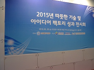 KAIST Exhibits Socially Benign Technologies
Exhibited 29 products that address the need to solve social issues such as a Braille printer
Students from the KAIST Idea Factory, a startup program for undergraduates operated by the Research Institute for Social Technology and Innovation (RISTI), hosted an exhibition presenting their research prototypes. The Idea Factory provides students with opportunities to try out new ideas and develop innovative technologies.
The exhibition was held at the Creative Learning building on campus on March 20, 2015. Students displayed 29 inventions, showcasing technologies to address important social issues. The exhibit included products and technologies developed by the students or already commercialized by small businesses such as a Braille printer, a hydrogen peroxide-oxygen respirator for vessel accidents, and an educational 3D printer. The small business exhibits included a removable additional power unit for wheelchairs, agricultural product anti-theft system, and security lighting.
KAIST also hosted a social technology innovation symposium in KAIST Institute Building on the same day. The theme of the symposium was the “Integration of Technological Innovation and Social Innovation – Social Technology Innovation.”
The key note speaker, Director Heung-Kyu Lee of RISTI, KAIST, presented a lecture on the topic, “The Meaning of Social Technology Innovation: System Change.” His talk was followed by Hyuk-Jin Choi of the Korea Social Enterprise Promotion Agency on “Social Economic Organizations of Korea and Social Technology,” and Jae-Sun Kim of The Grassroots on “Search for Social Innovation and Social Economy.”
The supervisor of the event, Director Lee said, “This exhibit focuses on technologies that could help the underprivileged. We will continue to support students’ ideas and small businesses’ endeavors to develop these technologies.”
KAIST established the Idea Factory in 2014 to assist KAIST students to commercialize creative and innovative ideas. The Idea Factory made a key contribution in commercializing the educational 3D printers last year.
Picture: A Braille Printer
2015.03.20 View 7867
KAIST Exhibits Socially Benign Technologies
Exhibited 29 products that address the need to solve social issues such as a Braille printer
Students from the KAIST Idea Factory, a startup program for undergraduates operated by the Research Institute for Social Technology and Innovation (RISTI), hosted an exhibition presenting their research prototypes. The Idea Factory provides students with opportunities to try out new ideas and develop innovative technologies.
The exhibition was held at the Creative Learning building on campus on March 20, 2015. Students displayed 29 inventions, showcasing technologies to address important social issues. The exhibit included products and technologies developed by the students or already commercialized by small businesses such as a Braille printer, a hydrogen peroxide-oxygen respirator for vessel accidents, and an educational 3D printer. The small business exhibits included a removable additional power unit for wheelchairs, agricultural product anti-theft system, and security lighting.
KAIST also hosted a social technology innovation symposium in KAIST Institute Building on the same day. The theme of the symposium was the “Integration of Technological Innovation and Social Innovation – Social Technology Innovation.”
The key note speaker, Director Heung-Kyu Lee of RISTI, KAIST, presented a lecture on the topic, “The Meaning of Social Technology Innovation: System Change.” His talk was followed by Hyuk-Jin Choi of the Korea Social Enterprise Promotion Agency on “Social Economic Organizations of Korea and Social Technology,” and Jae-Sun Kim of The Grassroots on “Search for Social Innovation and Social Economy.”
The supervisor of the event, Director Lee said, “This exhibit focuses on technologies that could help the underprivileged. We will continue to support students’ ideas and small businesses’ endeavors to develop these technologies.”
KAIST established the Idea Factory in 2014 to assist KAIST students to commercialize creative and innovative ideas. The Idea Factory made a key contribution in commercializing the educational 3D printers last year.
Picture: A Braille Printer
2015.03.20 View 7867 -
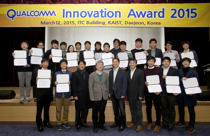 Qualcomm Innovation Award Recognizes 20 KAIST Students
The
award provides research fellowships, worth of USD 100,000, to 20 KAIST graduate
students
With an audience of 100 people present,
KAIST held a ceremony for the Qualcomm Innovation Award 2015 at the Information
Technology Convergence building on campus on March 12, 2015.
The Qualcomm Innovation Award, established
in 2010, is a fellowship that supports innovative science and engineering master’s
and doctoral students at KAIST. Qualcomm donated USD 100,000 to KAIST, stipulating that it be used to foster a creative research environment for graduate
students.
To select the recipients, KAIST formed an award committee chaired
by Professor Soo-Young Lee of the Department of Electrical Engineering and accepted research proposals until late January.
The award committee first selected 37
proposals from 75 papers submitted and then chose the final 20 research
proposals on March 12, 2015 after presentation evaluations. The presentations had to show promise of innovation and creativity; prospective influence on wireless communications
and mobile industry; and the prospect of being implemented.
Each recipient received a USD 4,500 research
fellowship along with an opportunity to present their research findings at a
workshop where Qualcomm engineers and other distinguished individuals of the industry
will attend.
Previously, Qualcomm has donated
research fellowships to KAIST graduate students in 2011 and 2013.
2015.03.19 View 10907
Qualcomm Innovation Award Recognizes 20 KAIST Students
The
award provides research fellowships, worth of USD 100,000, to 20 KAIST graduate
students
With an audience of 100 people present,
KAIST held a ceremony for the Qualcomm Innovation Award 2015 at the Information
Technology Convergence building on campus on March 12, 2015.
The Qualcomm Innovation Award, established
in 2010, is a fellowship that supports innovative science and engineering master’s
and doctoral students at KAIST. Qualcomm donated USD 100,000 to KAIST, stipulating that it be used to foster a creative research environment for graduate
students.
To select the recipients, KAIST formed an award committee chaired
by Professor Soo-Young Lee of the Department of Electrical Engineering and accepted research proposals until late January.
The award committee first selected 37
proposals from 75 papers submitted and then chose the final 20 research
proposals on March 12, 2015 after presentation evaluations. The presentations had to show promise of innovation and creativity; prospective influence on wireless communications
and mobile industry; and the prospect of being implemented.
Each recipient received a USD 4,500 research
fellowship along with an opportunity to present their research findings at a
workshop where Qualcomm engineers and other distinguished individuals of the industry
will attend.
Previously, Qualcomm has donated
research fellowships to KAIST graduate students in 2011 and 2013.
2015.03.19 View 10907 -
 Professor Sangyong Jon Appointed Fellow of AIMBE
Professor Sangyong Jon of the Department of Biological Sciences at KAIST has been appointed a member of the American Institute for Medical and Biological Engineering (AIMBE) fellowship.
Established in 1991, AIMBE is a non-profit organization based in Washington, D.C., representing 50,000 individuals and the top 2% of medical and biological engineers. AIMBE provides policy advice and advocacy for medical and biological engineering for the benefit of humanity. It has had about 1,500 fellows over the past 25 years. Among the members, only 110 are non-American nationalities.
Following the appointment of Dr. Hae-Bang Lee, the former senior researcher at the Korean Research Institute of Chemical Technology, and Distinguished Professor Sang Yup Lee of the Department of Chemical and Biomolecular Engineering at KAIST, Professor Jon is the third Korean to become an AIMBE fellow. He had an induction ceremony for the appointment of his fellowship at the AIMBE’s Annual Event held on March 15-17, 2015 in Washington, D.C.
An authority on nanomedicine, Professor Jon has developed many original technologies including multi-functional Theranostics nano particles for the diagnosis and treatment of diseases. He received the Most Cited Paper Award from Theranostics, an academic journal specialized in nanomedicine, last February.
Additionally, Professor Jon is a leading researcher in the field of translational medicine, using a multi-disciplinary, highly collaborative, “Bench to Bedside” approach for disease treatment and prevention. He created a biotechnology venture company and transferred research developments to the industry in Korea.
2015.03.12 View 13737
Professor Sangyong Jon Appointed Fellow of AIMBE
Professor Sangyong Jon of the Department of Biological Sciences at KAIST has been appointed a member of the American Institute for Medical and Biological Engineering (AIMBE) fellowship.
Established in 1991, AIMBE is a non-profit organization based in Washington, D.C., representing 50,000 individuals and the top 2% of medical and biological engineers. AIMBE provides policy advice and advocacy for medical and biological engineering for the benefit of humanity. It has had about 1,500 fellows over the past 25 years. Among the members, only 110 are non-American nationalities.
Following the appointment of Dr. Hae-Bang Lee, the former senior researcher at the Korean Research Institute of Chemical Technology, and Distinguished Professor Sang Yup Lee of the Department of Chemical and Biomolecular Engineering at KAIST, Professor Jon is the third Korean to become an AIMBE fellow. He had an induction ceremony for the appointment of his fellowship at the AIMBE’s Annual Event held on March 15-17, 2015 in Washington, D.C.
An authority on nanomedicine, Professor Jon has developed many original technologies including multi-functional Theranostics nano particles for the diagnosis and treatment of diseases. He received the Most Cited Paper Award from Theranostics, an academic journal specialized in nanomedicine, last February.
Additionally, Professor Jon is a leading researcher in the field of translational medicine, using a multi-disciplinary, highly collaborative, “Bench to Bedside” approach for disease treatment and prevention. He created a biotechnology venture company and transferred research developments to the industry in Korea.
2015.03.12 View 13737 -
 KAIST Develops Ultrathin Polymer Insulators Key to Low-Power Soft Electronics
Using an initiated chemical vapor deposition technique, the research team created an ultrathin polymeric insulating layer essential in realizing transistors with flexibility and low power consumption. This advance is expected to accelerate the commercialization of wearable and soft electronics.
A group of researchers at the Korea Advanced Institute of Science and Technology (KAIST) developed a high-performance ultrathin polymeric insulator for field-effect transistors (FETs). The researchers used vaporized monomers to form polymeric films grown conformally on various surfaces including plastics to produce a versatile insulator that meets a wide range of requirements for next-generation electronic devices. Their research results were published online in Nature Materials on March 9th, 2015.
FETs are an essential component for any modern electronic device used in our daily life from cell phones and computers, to flat-panel displays. Along with three electrodes (gate, source, and drain), FETs consist of an insulating layer and a semiconductor channel layer. The insulator in FETs plays an important role in controlling the conductance of the semiconductor channel and thus current flow within the translators. For reliable and low-power operation of FETs, electrically robust, ultrathin insulators are essential. Conventionally, such insulators are made of inorganic materials (e.g., oxides and nitrides) built on a hard surface such as silicon or glass due to their excellent insulating performance and reliability.
However, these insulators were difficult to implement into soft electronics due to their rigidity and high process temperature. In recent years, many researchers have studied polymers as promising insulating materials that are compatible with soft unconventional substrates and emerging semiconductor materials. The traditional technique employed in developing a polymer insulator, however, had the limitations of low surface coverage at ultra-low thickness, hindering FETs adopting polymeric insulators from operating at low voltage.
A KAIST research team led by Professor Sung Gap Im of the Chemical and Biomolecular Engineering Department and Professor Seunghyup Yoo and Professor Byung Jin Cho of the Electrical Engineering Department developed an insulating layer of organic polymers, “pV3D3,” that can be greatly scaled down, without losing its ideal insulating properties, to a thickness of less than 10 nanometers (nm) using the all-dry vapor-phase technique called the “initiated chemical vapor deposition (iCVD).”
The iCVD process allows gaseous monomers and initiators to react with each other in a low vacuum condition, and as a result, conformal polymeric films with excellent insulating properties are deposited on a substrate. Unlike the traditional technique, the surface-growing character of iCVD can overcome the problems associated with surface tension and produce highly uniform and pure ultrathin polymeric films over a large area with virtually no surface or substrate limitations. Furthermore, most iCVD polymers are created at room temperature, which lessens the strain exerted upon and damage done to the substrates.
With the pV3D3 insulator, the research team built low-power, high-performance FETs based on various semiconductor materials such as organics, graphene, and oxides, demonstrating the pV3D3 insulator’s wide range of material compatibility. They also manufactured a stick-on, removable electronic component using conventional packaging tape as a substrate. In collaboration with Professor Yong-Young Noh from Dongguk University in Korea, the team successfully developed a transistor array on a large-scale flexible substrate with the pV3D3 insulator.
Professor Im said, “The down-scalability and wide range of compatibility observed with iCVD-grown pV3D3 are unprecedented for polymeric insulators. Our iCVD pV3D3 polymeric films showed an insulating performance comparable to that of inorganic insulating layers, even when their thickness were scaled down to sub-10 nm. We expect our development will greatly benefit flexible or soft electronics, which will play a key role in the success of emerging electronic devices such as wearable computers.”
The title of the research paper is “Synthesis of ultrathin polymer insulating layers by initiated chemical vapor deposition for low-power soft electronics” (Digital Object Identifier (DOI) number is 10.1038/nmat4237).
Picture 1: A schematic image to show how the initiated chemical vapor deposition (iCVD) technique produces pV3D3 polymeric films: (i) introduction of vaporized monomers and initiators, (ii) activation of initiators to thermally dissociate into radicals, (iii) adsorption of monomers and initiator radicals onto a substrate, and (iv) transformation of free-radical polymerization into pV3D3 thin films.
Picture 2: This is a transistor array fabricated on a large scale, highly flexible substrate with pV3D3 polymeric films.
Picture 3: This photograph shows an electronic component fabricated on a conventional packaging tape, which is attachable or detachable, with pV3D3 polymeric films embedded.
2015.03.10 View 14180
KAIST Develops Ultrathin Polymer Insulators Key to Low-Power Soft Electronics
Using an initiated chemical vapor deposition technique, the research team created an ultrathin polymeric insulating layer essential in realizing transistors with flexibility and low power consumption. This advance is expected to accelerate the commercialization of wearable and soft electronics.
A group of researchers at the Korea Advanced Institute of Science and Technology (KAIST) developed a high-performance ultrathin polymeric insulator for field-effect transistors (FETs). The researchers used vaporized monomers to form polymeric films grown conformally on various surfaces including plastics to produce a versatile insulator that meets a wide range of requirements for next-generation electronic devices. Their research results were published online in Nature Materials on March 9th, 2015.
FETs are an essential component for any modern electronic device used in our daily life from cell phones and computers, to flat-panel displays. Along with three electrodes (gate, source, and drain), FETs consist of an insulating layer and a semiconductor channel layer. The insulator in FETs plays an important role in controlling the conductance of the semiconductor channel and thus current flow within the translators. For reliable and low-power operation of FETs, electrically robust, ultrathin insulators are essential. Conventionally, such insulators are made of inorganic materials (e.g., oxides and nitrides) built on a hard surface such as silicon or glass due to their excellent insulating performance and reliability.
However, these insulators were difficult to implement into soft electronics due to their rigidity and high process temperature. In recent years, many researchers have studied polymers as promising insulating materials that are compatible with soft unconventional substrates and emerging semiconductor materials. The traditional technique employed in developing a polymer insulator, however, had the limitations of low surface coverage at ultra-low thickness, hindering FETs adopting polymeric insulators from operating at low voltage.
A KAIST research team led by Professor Sung Gap Im of the Chemical and Biomolecular Engineering Department and Professor Seunghyup Yoo and Professor Byung Jin Cho of the Electrical Engineering Department developed an insulating layer of organic polymers, “pV3D3,” that can be greatly scaled down, without losing its ideal insulating properties, to a thickness of less than 10 nanometers (nm) using the all-dry vapor-phase technique called the “initiated chemical vapor deposition (iCVD).”
The iCVD process allows gaseous monomers and initiators to react with each other in a low vacuum condition, and as a result, conformal polymeric films with excellent insulating properties are deposited on a substrate. Unlike the traditional technique, the surface-growing character of iCVD can overcome the problems associated with surface tension and produce highly uniform and pure ultrathin polymeric films over a large area with virtually no surface or substrate limitations. Furthermore, most iCVD polymers are created at room temperature, which lessens the strain exerted upon and damage done to the substrates.
With the pV3D3 insulator, the research team built low-power, high-performance FETs based on various semiconductor materials such as organics, graphene, and oxides, demonstrating the pV3D3 insulator’s wide range of material compatibility. They also manufactured a stick-on, removable electronic component using conventional packaging tape as a substrate. In collaboration with Professor Yong-Young Noh from Dongguk University in Korea, the team successfully developed a transistor array on a large-scale flexible substrate with the pV3D3 insulator.
Professor Im said, “The down-scalability and wide range of compatibility observed with iCVD-grown pV3D3 are unprecedented for polymeric insulators. Our iCVD pV3D3 polymeric films showed an insulating performance comparable to that of inorganic insulating layers, even when their thickness were scaled down to sub-10 nm. We expect our development will greatly benefit flexible or soft electronics, which will play a key role in the success of emerging electronic devices such as wearable computers.”
The title of the research paper is “Synthesis of ultrathin polymer insulating layers by initiated chemical vapor deposition for low-power soft electronics” (Digital Object Identifier (DOI) number is 10.1038/nmat4237).
Picture 1: A schematic image to show how the initiated chemical vapor deposition (iCVD) technique produces pV3D3 polymeric films: (i) introduction of vaporized monomers and initiators, (ii) activation of initiators to thermally dissociate into radicals, (iii) adsorption of monomers and initiator radicals onto a substrate, and (iv) transformation of free-radical polymerization into pV3D3 thin films.
Picture 2: This is a transistor array fabricated on a large scale, highly flexible substrate with pV3D3 polymeric films.
Picture 3: This photograph shows an electronic component fabricated on a conventional packaging tape, which is attachable or detachable, with pV3D3 polymeric films embedded.
2015.03.10 View 14180 -
 The Real Time Observation of the Birth of a Molecule
From right to left: Dr. Kyung-Hwan Kim, Professor Hyotcherl Lhee, and Jong-Gu Kim, a Ph.D. candidate
Professor Hyotcherl Lhee of the Department of Chemistry at KAIST and Japanese research teams jointly published their research results showing that they have succeeded in the direct observation of how atoms form a molecule in the online issue of Nature on February 19, 2015.
The researchers used water in which gold atoms ([Au(CN) 2- ]) are dissolved and fired X-ray pulses over the specimen in femtosecond timescales to study chemical reactions taking place among the gold atoms. They were able to examine in real time the instant process of how gold atoms bond together to become a molecule, to a trimer or tetramer state.
This direct viewing of the formation of a gold trimer complex ([Au(CN) 2- ] 3 ) will provide an opportunity to understand complex chemical and biological systems.
For details, please see the following press release that was distributed by the High Energy Accelerator Research Organization, KEK, in Japan:
Direct Observation of Bond Formations
February 18, 2015
A collaboration between researchers from KEK, the Institute for Basic Science (IBS), the Korea Advanced Institute of Science and Technology (KAIST), RIKEN, and the Japan Synchrotron Radiation Research Institute (JASRI) used the SACLA X-ray free electron laser (XFEL) facility for a real time visualization of the birth of a molecular that occurs via photoinduced formation of a chemical bonds. This achievement was published in the online version of the scientific journal “Nature” (published on 19 February 2015).
Direct “observation” of the bond making, through a chemical reaction, has been longstanding dream for chemists. However, the distance between atoms is very small, at about 100 picometer, and the bonding is completed very quickly, taking less than one picosecond (ps). Hence, previously, one could only imagine the bond formation between atoms while looking at the chemical reaction progressing in the test-tube.
In this study, the research group focused on the process of photoinduced bond formation between gold (Au) ions dissolved in water. In the ground state (S 0 state in Fig. 1) Au ions that are weakly bound to each other by an electron affinity and aligned in a bent geometry. Upon a photoexcitation, the S 0 state rapidly converts into an excited (S 1 state in Fig. 1) state where Au-Au covalent bonds are formed among Au ions aligned in a linear geometry. Subsequently, the S 1 state transforms to a triplet state (T 1 state in Fig. 1) in 1.6 ps while accompanying further contraction of Au-Au bonds by 0.1 Å. Later, the T 1 state of the trimer converts to a tetramer (tetramer state in Fig. 1) on nanosecond time scale. Finally, the Au ions returned to their original loosely interacting bent structure.
In this research, the direct observation of a very fast chemical reaction, induced by the photo-excitation, was succeeded (Fig. 2, 3). Therefore, this method is expected to be a fundamental technology for understanding the light energy conversion reaction. The research group is actively working to apply this method to the development of viable renewable energy resources, such as a photocatalysts for artificial photosynthesis using sunlight.
This research was supported by the X-ray Free Electron Laser Priority Strategy Program of the MEXT, PRESTO of the JST, and the the Innovative Areas "Artificial Photosynthesis (AnApple)" grant from the Japan Society for the Promotion of Science (JSPS).
Publication: Nature , 518 (19 February 2015)
Title: Direct observation of bond formation in solution with femtosecond X-ray scattering
Authors: K. H. Kim 1 , J. G. Kim 1 , S. Nozawa 1 , T. Sato 1 , K. Y. Oang, T. W. Kim, H. Ki, J. Jo, S. Park, C. Song, T. Sato, K. Ogawa, T. Togashi, K. Tono, M. Yabashi, T. Ishikawa, J. Kim, R. Ryoo, J. Kim, H. Ihee, S. Adachi. ※ 1: These authors contributed equally to the work.
DOI: 10.1038/nature14163
Figure 1. Structure of a gold cyano trimer complex (Au(CN) 2 - ) 3 .
Figure 2. Observed changes in the molecular structure of the gold complex
Figure 3. Schematic view of the research of photo-chemical reactions by the molecular movie
2015.02.27 View 13508
The Real Time Observation of the Birth of a Molecule
From right to left: Dr. Kyung-Hwan Kim, Professor Hyotcherl Lhee, and Jong-Gu Kim, a Ph.D. candidate
Professor Hyotcherl Lhee of the Department of Chemistry at KAIST and Japanese research teams jointly published their research results showing that they have succeeded in the direct observation of how atoms form a molecule in the online issue of Nature on February 19, 2015.
The researchers used water in which gold atoms ([Au(CN) 2- ]) are dissolved and fired X-ray pulses over the specimen in femtosecond timescales to study chemical reactions taking place among the gold atoms. They were able to examine in real time the instant process of how gold atoms bond together to become a molecule, to a trimer or tetramer state.
This direct viewing of the formation of a gold trimer complex ([Au(CN) 2- ] 3 ) will provide an opportunity to understand complex chemical and biological systems.
For details, please see the following press release that was distributed by the High Energy Accelerator Research Organization, KEK, in Japan:
Direct Observation of Bond Formations
February 18, 2015
A collaboration between researchers from KEK, the Institute for Basic Science (IBS), the Korea Advanced Institute of Science and Technology (KAIST), RIKEN, and the Japan Synchrotron Radiation Research Institute (JASRI) used the SACLA X-ray free electron laser (XFEL) facility for a real time visualization of the birth of a molecular that occurs via photoinduced formation of a chemical bonds. This achievement was published in the online version of the scientific journal “Nature” (published on 19 February 2015).
Direct “observation” of the bond making, through a chemical reaction, has been longstanding dream for chemists. However, the distance between atoms is very small, at about 100 picometer, and the bonding is completed very quickly, taking less than one picosecond (ps). Hence, previously, one could only imagine the bond formation between atoms while looking at the chemical reaction progressing in the test-tube.
In this study, the research group focused on the process of photoinduced bond formation between gold (Au) ions dissolved in water. In the ground state (S 0 state in Fig. 1) Au ions that are weakly bound to each other by an electron affinity and aligned in a bent geometry. Upon a photoexcitation, the S 0 state rapidly converts into an excited (S 1 state in Fig. 1) state where Au-Au covalent bonds are formed among Au ions aligned in a linear geometry. Subsequently, the S 1 state transforms to a triplet state (T 1 state in Fig. 1) in 1.6 ps while accompanying further contraction of Au-Au bonds by 0.1 Å. Later, the T 1 state of the trimer converts to a tetramer (tetramer state in Fig. 1) on nanosecond time scale. Finally, the Au ions returned to their original loosely interacting bent structure.
In this research, the direct observation of a very fast chemical reaction, induced by the photo-excitation, was succeeded (Fig. 2, 3). Therefore, this method is expected to be a fundamental technology for understanding the light energy conversion reaction. The research group is actively working to apply this method to the development of viable renewable energy resources, such as a photocatalysts for artificial photosynthesis using sunlight.
This research was supported by the X-ray Free Electron Laser Priority Strategy Program of the MEXT, PRESTO of the JST, and the the Innovative Areas "Artificial Photosynthesis (AnApple)" grant from the Japan Society for the Promotion of Science (JSPS).
Publication: Nature , 518 (19 February 2015)
Title: Direct observation of bond formation in solution with femtosecond X-ray scattering
Authors: K. H. Kim 1 , J. G. Kim 1 , S. Nozawa 1 , T. Sato 1 , K. Y. Oang, T. W. Kim, H. Ki, J. Jo, S. Park, C. Song, T. Sato, K. Ogawa, T. Togashi, K. Tono, M. Yabashi, T. Ishikawa, J. Kim, R. Ryoo, J. Kim, H. Ihee, S. Adachi. ※ 1: These authors contributed equally to the work.
DOI: 10.1038/nature14163
Figure 1. Structure of a gold cyano trimer complex (Au(CN) 2 - ) 3 .
Figure 2. Observed changes in the molecular structure of the gold complex
Figure 3. Schematic view of the research of photo-chemical reactions by the molecular movie
2015.02.27 View 13508 -
 KAIST Develops Subminiature, Power-Efficient Air Pollution Sensing Probe
Professor Inkyu Park and his research team from the Department of Mechanical Engineering at KAIST have developed a subminiature, power-efficient air-pollution sensing probe that can be applied to mobile devices. Their research findings were published online in the January 30th issue of Scientific Reports.
As air pollution has increased, people have taken greater interest in health care. The developed technology could allow people to measure independently the air pollution level of their surrounding environments.
Previous instruments used to measure air pollution levels were bulky and consumed a lot of power. They also often produced inaccurate results when measuring air pollution in which different toxic gases were mixed. These problems could not be resolved with existing semiconductor manufacturing process.
Using local temperature field control technology, Professor Park’s team succeeded in integrating multiple heterogeneous nanomaterials and fitting them onto a small, low-power electronic chip. This microheating sensor can heat microscale regions through local hydrothermal synthesis. Because it requires a miniscale amount of nanomaterials to manufacture, the sensor is most suitable for mobile devices.
Professor Park said, “Our research will contribute to the development of convergence technology in such field as air pollution sensing probes, biosensors, electronic devices, and displays.”
The team's research was supported by the Ministry of Education and the Ministry of Science, ICT and Future Planning, Republic of Korea.
Figure 1 – The Concept of Multiple Nanomaterial Device and Numerical Simulation Results of Precursor Solutions
Figure 2 - Multiple Nanomaterial Manufactured in a Microscale Region
2015.02.27 View 11694
KAIST Develops Subminiature, Power-Efficient Air Pollution Sensing Probe
Professor Inkyu Park and his research team from the Department of Mechanical Engineering at KAIST have developed a subminiature, power-efficient air-pollution sensing probe that can be applied to mobile devices. Their research findings were published online in the January 30th issue of Scientific Reports.
As air pollution has increased, people have taken greater interest in health care. The developed technology could allow people to measure independently the air pollution level of their surrounding environments.
Previous instruments used to measure air pollution levels were bulky and consumed a lot of power. They also often produced inaccurate results when measuring air pollution in which different toxic gases were mixed. These problems could not be resolved with existing semiconductor manufacturing process.
Using local temperature field control technology, Professor Park’s team succeeded in integrating multiple heterogeneous nanomaterials and fitting them onto a small, low-power electronic chip. This microheating sensor can heat microscale regions through local hydrothermal synthesis. Because it requires a miniscale amount of nanomaterials to manufacture, the sensor is most suitable for mobile devices.
Professor Park said, “Our research will contribute to the development of convergence technology in such field as air pollution sensing probes, biosensors, electronic devices, and displays.”
The team's research was supported by the Ministry of Education and the Ministry of Science, ICT and Future Planning, Republic of Korea.
Figure 1 – The Concept of Multiple Nanomaterial Device and Numerical Simulation Results of Precursor Solutions
Figure 2 - Multiple Nanomaterial Manufactured in a Microscale Region
2015.02.27 View 11694 -
 KAIST's Thermoelectric Generator on Glass Fabric Receives the Grand Prize at the Netexplo Forum 2015
The forum announced top ten IT innovations expected to change the world and selected the grand prize on February 4, 2014.
Established in 2007 by Martine Bidegain and Thierry Happe in partnership with the French Senate and the French Ministry for the Digital Economy, the Netexplo Observatory is an independent global organization that studies the impact of digital technology and innovation on society and business.
Every year, the Netexplo Observatory hosts an international conference, the Netexplo Forum, in Paris, France, which surveys digital innovation worldwide. The 8th forum was held in partnership with the United Nations Educational, Scientific and Cultural Organization (UNESCO) on February 4-5, 2015, at the UNESCO House in Paris.
Prior to the conference, the Netexplo Forum 2015 named the top ten most promising digital technologies that will greatly impact the world.
Among them was Professor Byung Jin Cho’s research on a wearable thermoelectric generator (http://www.eurekalert.org/pub_releases/2014-04/tkai-tgo041014.php). The generator was selected as the most innovative technology this year.
Professor Cho of KAIST’s Electrical Engineering Department developed a glass fabric-based thermoelectric generator that is extremely light and flexible and that produces electricity from the heat of the human body. This technology can be applied widely to wearable computers and mobile devices.
The full list of innovations follows below:
Wearable Thermo-Element, South Korea: The human body becomes a source of energy for mobile devices.
W.Afate 3D-printer, Togo: An environmentally friendly fablab that makes a low-cost 3D-printer from recycling electronic components.
Slack, USA: By combining email, Skype, and file-sharing and social networks, internal communication becomes much easier and simpler.
PhotoMath, Croatia: A free app that enables smartphone users to solve mathematical problems simply by scanning the mathematical texts.
Kappo, Chile: Connected cyclists produce and transmit useful data for urban planning to make the city more bike-friendly.
Branching Minds, USA: An improved learning process for students in difficulty through a personalized approach.
Baidu Kuai Sou, China: Smart chopsticks that can check food hazards.
SCio, Israel: A pocket molecular sensor with various applications and data
Rainforest Connection, USA: Fighting deforestation with recycled smartphones
Sense Ebola Followup, Nigeria: A mobile tool to help contain Ebola
For more details on the wearable thermos-element which received the 2015 Netexplo Award, please go to https://www.netexplo.org/en/intelligence/innovation/wearable-thermo-element.
Pictures 1 and 2: A high-performance wearable thermoelectric generator that is extremely flexible and light.
Picture 3: Senator Catherine Morin-Desailly (left) of the French Parliament presents the 2015 Netexplo Award to Professor Byung Jin Cho (right) on February 4, 2015 at the UNESCO House in Paris.
Credit of Loran Dhérines
Picture 4: Professor Byung Jin Cho (left) poses with Dr. Joël de Rosnay (right).
Credit of Loran Dhérines
2015.02.06 View 15437
KAIST's Thermoelectric Generator on Glass Fabric Receives the Grand Prize at the Netexplo Forum 2015
The forum announced top ten IT innovations expected to change the world and selected the grand prize on February 4, 2014.
Established in 2007 by Martine Bidegain and Thierry Happe in partnership with the French Senate and the French Ministry for the Digital Economy, the Netexplo Observatory is an independent global organization that studies the impact of digital technology and innovation on society and business.
Every year, the Netexplo Observatory hosts an international conference, the Netexplo Forum, in Paris, France, which surveys digital innovation worldwide. The 8th forum was held in partnership with the United Nations Educational, Scientific and Cultural Organization (UNESCO) on February 4-5, 2015, at the UNESCO House in Paris.
Prior to the conference, the Netexplo Forum 2015 named the top ten most promising digital technologies that will greatly impact the world.
Among them was Professor Byung Jin Cho’s research on a wearable thermoelectric generator (http://www.eurekalert.org/pub_releases/2014-04/tkai-tgo041014.php). The generator was selected as the most innovative technology this year.
Professor Cho of KAIST’s Electrical Engineering Department developed a glass fabric-based thermoelectric generator that is extremely light and flexible and that produces electricity from the heat of the human body. This technology can be applied widely to wearable computers and mobile devices.
The full list of innovations follows below:
Wearable Thermo-Element, South Korea: The human body becomes a source of energy for mobile devices.
W.Afate 3D-printer, Togo: An environmentally friendly fablab that makes a low-cost 3D-printer from recycling electronic components.
Slack, USA: By combining email, Skype, and file-sharing and social networks, internal communication becomes much easier and simpler.
PhotoMath, Croatia: A free app that enables smartphone users to solve mathematical problems simply by scanning the mathematical texts.
Kappo, Chile: Connected cyclists produce and transmit useful data for urban planning to make the city more bike-friendly.
Branching Minds, USA: An improved learning process for students in difficulty through a personalized approach.
Baidu Kuai Sou, China: Smart chopsticks that can check food hazards.
SCio, Israel: A pocket molecular sensor with various applications and data
Rainforest Connection, USA: Fighting deforestation with recycled smartphones
Sense Ebola Followup, Nigeria: A mobile tool to help contain Ebola
For more details on the wearable thermos-element which received the 2015 Netexplo Award, please go to https://www.netexplo.org/en/intelligence/innovation/wearable-thermo-element.
Pictures 1 and 2: A high-performance wearable thermoelectric generator that is extremely flexible and light.
Picture 3: Senator Catherine Morin-Desailly (left) of the French Parliament presents the 2015 Netexplo Award to Professor Byung Jin Cho (right) on February 4, 2015 at the UNESCO House in Paris.
Credit of Loran Dhérines
Picture 4: Professor Byung Jin Cho (left) poses with Dr. Joël de Rosnay (right).
Credit of Loran Dhérines
2015.02.06 View 15437 -
 Dr. Hak-Min Kim Appointed New KAIST Auditor
KAIST’s Board of Trustees appointed Dr. Hak-Min Kim the new auditor for the university on January 30, 2015 at the K Hotel in Seoul. Dr. Kim will serve from January 30, 2015 to January 29, 2018.
A bachelor's graduate of the Metallurgical Engineering Department at Seoul National University, Dr. Kim received his master’s and doctoral degrees from Carnegie Mellon University in the United States. He returned to Korea in the early 1980s and worked for the Korea Institute of Machinery and Materials (KIMM), the Korea Institute of Science and Technology Evaluation and Planning, and the Ministry of Science, ICT and Future Planning, the Republic of Korea.
Since 2012, Dr. Kim has been serving the Research Committee at the Korea Institute of Materials Science, an affiliation of KIMM.
2015.02.06 View 7227
Dr. Hak-Min Kim Appointed New KAIST Auditor
KAIST’s Board of Trustees appointed Dr. Hak-Min Kim the new auditor for the university on January 30, 2015 at the K Hotel in Seoul. Dr. Kim will serve from January 30, 2015 to January 29, 2018.
A bachelor's graduate of the Metallurgical Engineering Department at Seoul National University, Dr. Kim received his master’s and doctoral degrees from Carnegie Mellon University in the United States. He returned to Korea in the early 1980s and worked for the Korea Institute of Machinery and Materials (KIMM), the Korea Institute of Science and Technology Evaluation and Planning, and the Ministry of Science, ICT and Future Planning, the Republic of Korea.
Since 2012, Dr. Kim has been serving the Research Committee at the Korea Institute of Materials Science, an affiliation of KIMM.
2015.02.06 View 7227 -
 KAIST Develops a Method to Transfer Graphene by Stamping
Professor Sung-Yool Choi’s research team from KAIST's Department of Electrical Engineering has developed a technique that can produce a single-layer graphene from a metal etching. Through this, transferring a graphene layer onto a circuit board can be done as easily as stamping a seal on paper.
The research findings were published in the January 14th issue of Small as the lead article.
This technology will allow different types of wafer transfer methods such as transfer onto a surface of a device or a curved surface, and large surface transfer onto a 4 inch wafer. It will be applied in the field of wearable smart gadgets through commercialization of graphene electronic devices.
The traditional method used to transfer graphene onto a circuit board is a wet transfer. However, it has some drawbacks as the graphene layer can be damaged or contaminated during the transfer process from residue from the metal etching. This may affect the electrical properties of the transferred graphene.
After a graphene growth substrate formed on a catalytic metal substrate is pretreated in an aqueous poly vinyl alcohol (PVA) solution, a PVA film forms on the pretreated substrate. The substrate and the graphene layers bond strongly. The graphene is lifted from the growth substrate by means of an elastomeric stamp.
The delaminated graphene layer is isolated state from the elastomeric stamp and thus can be freely transferred onto a circuit board. As the catalytic metal substrate can be reused and does not contain harmful chemical substances, such transfer method is very eco-friendly.
Professor Choi said, “As the new graphene transfer method has a wide range of applications and allows a large surface transfer, it will contribute to the commercialization of graphene electronic devices.” He added that “because this technique has a high degree of freedom in transfer process, it has a variety of usages for graphene and 2 dimensional nano-devices.”
This research was sponsored by the Ministry of Science, ICT and Future Planning, the Republic of Korea.
Figure 1. Cover photo of the journal Small which illustrates the research findings
Figure 2. Above view of Graphene layer transferred through the new method
Figure 3. Large surface transfer of Graphene
2015.01.23 View 12091
KAIST Develops a Method to Transfer Graphene by Stamping
Professor Sung-Yool Choi’s research team from KAIST's Department of Electrical Engineering has developed a technique that can produce a single-layer graphene from a metal etching. Through this, transferring a graphene layer onto a circuit board can be done as easily as stamping a seal on paper.
The research findings were published in the January 14th issue of Small as the lead article.
This technology will allow different types of wafer transfer methods such as transfer onto a surface of a device or a curved surface, and large surface transfer onto a 4 inch wafer. It will be applied in the field of wearable smart gadgets through commercialization of graphene electronic devices.
The traditional method used to transfer graphene onto a circuit board is a wet transfer. However, it has some drawbacks as the graphene layer can be damaged or contaminated during the transfer process from residue from the metal etching. This may affect the electrical properties of the transferred graphene.
After a graphene growth substrate formed on a catalytic metal substrate is pretreated in an aqueous poly vinyl alcohol (PVA) solution, a PVA film forms on the pretreated substrate. The substrate and the graphene layers bond strongly. The graphene is lifted from the growth substrate by means of an elastomeric stamp.
The delaminated graphene layer is isolated state from the elastomeric stamp and thus can be freely transferred onto a circuit board. As the catalytic metal substrate can be reused and does not contain harmful chemical substances, such transfer method is very eco-friendly.
Professor Choi said, “As the new graphene transfer method has a wide range of applications and allows a large surface transfer, it will contribute to the commercialization of graphene electronic devices.” He added that “because this technique has a high degree of freedom in transfer process, it has a variety of usages for graphene and 2 dimensional nano-devices.”
This research was sponsored by the Ministry of Science, ICT and Future Planning, the Republic of Korea.
Figure 1. Cover photo of the journal Small which illustrates the research findings
Figure 2. Above view of Graphene layer transferred through the new method
Figure 3. Large surface transfer of Graphene
2015.01.23 View 12091 -
 President Kang to Present at the World Economic Forum
President Sung-Mo Kang of KAIST will attend the World Economic Forum (WEF) as a member of the Global University Leaders Forum (GULF) to represent KAIST. GULF is attended by the world leaders of education and research. Its members represent 26 universities drawn from around the world including Harvard University. KAIST is the only Korean university to be invited.
WEF will be held in Davos, Switzerland, for four days, starting on 21 January 2015. He will discuss the future of higher education, the issues and solutions of science and society at GULF.
By attending GULF, KAIST expects to strengthen its network with top universities around the world and raise KAIST’s profile on an international basis. President Kang said, “The invitation for KAIST to attend the GULF is an evidence of its raised global status.” He continued, “I will show the innovative and challenging achievements KAIST has made to the leaders of the world.”
The theme of the 2015 World Economic Forum Annual Meeting 2015 is “The New Global Context” to discuss the integration of economic growth and society, employment and work force, environment and resource scarcity, the future of the Internet, and international crime and anti-corruption.
The World Economic Forum was established in 1971 by Klaus Schwab who is also its Executive Chairman. More than 2,500 people including German Chancellor Angela Merkel, French President François Hollande, Chinese Premier Li Keqiang, Google President Eric Schmidt, and Microsoft CEO Satya Nadella will attend this year's forum.
2015.01.22 View 9347
President Kang to Present at the World Economic Forum
President Sung-Mo Kang of KAIST will attend the World Economic Forum (WEF) as a member of the Global University Leaders Forum (GULF) to represent KAIST. GULF is attended by the world leaders of education and research. Its members represent 26 universities drawn from around the world including Harvard University. KAIST is the only Korean university to be invited.
WEF will be held in Davos, Switzerland, for four days, starting on 21 January 2015. He will discuss the future of higher education, the issues and solutions of science and society at GULF.
By attending GULF, KAIST expects to strengthen its network with top universities around the world and raise KAIST’s profile on an international basis. President Kang said, “The invitation for KAIST to attend the GULF is an evidence of its raised global status.” He continued, “I will show the innovative and challenging achievements KAIST has made to the leaders of the world.”
The theme of the 2015 World Economic Forum Annual Meeting 2015 is “The New Global Context” to discuss the integration of economic growth and society, employment and work force, environment and resource scarcity, the future of the Internet, and international crime and anti-corruption.
The World Economic Forum was established in 1971 by Klaus Schwab who is also its Executive Chairman. More than 2,500 people including German Chancellor Angela Merkel, French President François Hollande, Chinese Premier Li Keqiang, Google President Eric Schmidt, and Microsoft CEO Satya Nadella will attend this year's forum.
2015.01.22 View 9347 -
 An Advanced Method of DNA Nanostructure Formation Developed
Professor Tae-Young Yoon’s research team from the Department of Physics at KAIST has developed a new method to form DNA nanostructures by using magnetic tweezers to observe and to induce the formation of the structure in real time.
Unlike traditional designs of "DNA origami" which relies on thermal or chemical annealing methods, the new technology utilizes a completely different dynamic in DNA folding. This allows the folding to be done within only ten minutes.
Developed in 2006, the "DNA origami" allows a long skeleton of DNA to be folded into an arbitrary structure by using small stapler DNA pieces. This has been a prominent method in DNA nanotechnology.
However, the traditional technology which adopts thermal processes could not control the DNA formation during the folding because every interaction among DNAs occurs simultaneously. Thus, the thermal processes, which take dozens of hours to complete, had to be repeated multiple times in order to find the optimal condition.
The research team designed a DNA folding using uni-molecular magnetic tweezers that applied force to a single DNA molecule while measuring the state of the DNA. Through this technology, they were able to induce the formation of DNA nanostructure and observe it at the same time.
During high temperature heat treatment, the first stage of conventional thermal processes, the internal structure of the long skeleton DNA untangles. To induce such state, after attaching one side of the skeleton DNA to the surface of glass and the other side to a magnetic material, the team unfolded the internal structure of the DNA by pulling the two sides apart with magnetic force.
Unlike the conventional thermal processes, this method lets the stapler DNA swiftly adhere to the skeleton DNA within a minute because the sites are revealed at room temperature.
After the stapler pieces connected to the skeleton, the team removed the magnetic force. Next, the structure folded through self-assembly as the stapler DNAs stuck to different sites on the skeleton DNA.
Professor Yoon said, “With the existing thermal methods, we could not differentiate the reactions of the DNA because the response of each DNA pieces mutually interacted with each other.” He added that “Using the magnetic tweezers, we were able to sort the process of DNA nanostructure formation into a series of reactions of DNA molecules that are well known, and shorten the time taken for formation in only ten minutes.”
He commented, “This nanostructure formation method will enable us to create more intricate and desirable DNA nanostructures by programming the folding of DNA origami structures.”
Conducted by Dr. Woori Bae under the guidance of Professor Yoon, the research findings were published online in the December 4th issue of Nature Communications.
Figure 1: Uni-molecular magnetic tweezers orchestrating the DNA nanostructure formation
Figure 2: The evolution of DNA nanostructure formation using magnetic tweezers. The DNA nanostructure with a 21-nanometer size was formed in about eight minutes.
2015.01.06 View 7868
An Advanced Method of DNA Nanostructure Formation Developed
Professor Tae-Young Yoon’s research team from the Department of Physics at KAIST has developed a new method to form DNA nanostructures by using magnetic tweezers to observe and to induce the formation of the structure in real time.
Unlike traditional designs of "DNA origami" which relies on thermal or chemical annealing methods, the new technology utilizes a completely different dynamic in DNA folding. This allows the folding to be done within only ten minutes.
Developed in 2006, the "DNA origami" allows a long skeleton of DNA to be folded into an arbitrary structure by using small stapler DNA pieces. This has been a prominent method in DNA nanotechnology.
However, the traditional technology which adopts thermal processes could not control the DNA formation during the folding because every interaction among DNAs occurs simultaneously. Thus, the thermal processes, which take dozens of hours to complete, had to be repeated multiple times in order to find the optimal condition.
The research team designed a DNA folding using uni-molecular magnetic tweezers that applied force to a single DNA molecule while measuring the state of the DNA. Through this technology, they were able to induce the formation of DNA nanostructure and observe it at the same time.
During high temperature heat treatment, the first stage of conventional thermal processes, the internal structure of the long skeleton DNA untangles. To induce such state, after attaching one side of the skeleton DNA to the surface of glass and the other side to a magnetic material, the team unfolded the internal structure of the DNA by pulling the two sides apart with magnetic force.
Unlike the conventional thermal processes, this method lets the stapler DNA swiftly adhere to the skeleton DNA within a minute because the sites are revealed at room temperature.
After the stapler pieces connected to the skeleton, the team removed the magnetic force. Next, the structure folded through self-assembly as the stapler DNAs stuck to different sites on the skeleton DNA.
Professor Yoon said, “With the existing thermal methods, we could not differentiate the reactions of the DNA because the response of each DNA pieces mutually interacted with each other.” He added that “Using the magnetic tweezers, we were able to sort the process of DNA nanostructure formation into a series of reactions of DNA molecules that are well known, and shorten the time taken for formation in only ten minutes.”
He commented, “This nanostructure formation method will enable us to create more intricate and desirable DNA nanostructures by programming the folding of DNA origami structures.”
Conducted by Dr. Woori Bae under the guidance of Professor Yoon, the research findings were published online in the December 4th issue of Nature Communications.
Figure 1: Uni-molecular magnetic tweezers orchestrating the DNA nanostructure formation
Figure 2: The evolution of DNA nanostructure formation using magnetic tweezers. The DNA nanostructure with a 21-nanometer size was formed in about eight minutes.
2015.01.06 View 7868 -
 How Science Understands the Beauty of Fine Arts from the Medieval Era to the 19th Century
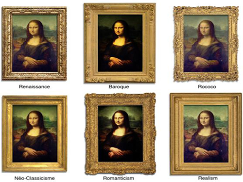
A research team, consisting of Professor Hawoong Jeong of the Department of Physics at KAIST and Assistant Professor Seung-Woo Son of the Department of Applied Physics at Hanyang University, conducted a research project to understand visual representations through the eyes of science, i.e., quantitative analyses. Researchers took a sample of reproductions of European paintings from the 11th to the early 19th centuries and analyzed them based on three elements: the usage of color, the variety of painted colors, and the brightness of the images.
For the large-scale quantitative analysis, the research team utilized digital images of the paintings obtained from the Web Gallery of Art, a virtual museum and searchable database of European fine arts that includes over 29,000 pieces, ranging from the years 1000 to 1850. The Web Gallery classifies paintings into ten art historical periods such as Medieval, Renaissance, Mannerist, Baroque, Rococo, Romantic, and Realist.
For each period, researchers investigated the frequency of certain colors which appear in paintings and examined the variety of painted colors, paying particular attention to paintings created by two iconoclastic artists from different eras: Pieter Bruegel the Elder and Jackson Pollock. In their works, the researchers discovered that specific pigments were preferred in each period, the result of reflecting historical facts into fine arts. For example, certain rare colors were used in the medieval age for political and religious reasons, and artists in that era employed a technique to layer one color over another dry color in order to express mixed colors, resulting in thickly textured brushstrokes because they considered mixing colors impure. Moreover, oil colors and color mixing techniques were not fully developed until the Renaissance age.
According to the research team, fewer numbers of colors were used before the 20th century, and the introduction of new expressionist tools, like the use of pastels and fingers directly on canvas, and painting techniques, such as “chiaroscuro” and “sfumato,” made much more colorful and natural expressions possible after the Renaissance period. The team said that the color arrangement of Jackson Pollock’s drip paintings differed substantially from other paintings, showing randomness, especially in the spatial arrangement of colors.
Researchers also examined one of the artistic effects applied to paintings, contrast, an important element to express shape and space in two dimensional fine arts. Among various types of contrasts, they said, brightness contrast is the most important in art history due to the cultural background of Europe which usually adopts the contrast of light and darkness as a metaphorical expression. Taking the color information of pixels and their spatial arrangement, the researchers studied the prevalence of brightness contrast in European paintings over ten artistic periods by developing a correlation function to measure the contrast. These mathematical measurements quantitatively describe the birth of new painting techniques including chiaroscuro and sfumato and their increasing use. For instance, in the medieval age, the contour of objects or images in paintings was vague, but it became much clearer later in the Romantic period.
Professor Jeong said, “The complexity of the material world has been a long-lasting topic of interest in natural science, but research in the structural complexity of art and humanities has only begun since the development of the Internet, with the availability of big data in these fields. Our research is a meaningful attempt to understand the underling intricacy of art and humanities based on a scientific approach, expressed quantitatively.”
The research results were published online on December 11, 2014 in Scientific Reports, entitled “Large-Scale Quantitative Analysis of Painting Arts.” The paper was also selected as one of the weekly research highlights by Nature and is noted on its online journal’s website.
YouTube link on “the brightness contrast”: http://youtu.be/SFo0h1EU2aw
Figure 1: Constructing brightness surfaces and measuring roughness exponents
Figure 2: Visual representations of Mona Lisa painted by Leonardo da Vinci, which was reproduced in accordance with the art historical periods
Figure 3: The screenshot of Nature online webpage
2014.12.23 View 9080
How Science Understands the Beauty of Fine Arts from the Medieval Era to the 19th Century
A research team, consisting of Professor Hawoong Jeong of the Department of Physics at KAIST and Assistant Professor Seung-Woo Son of the Department of Applied Physics at Hanyang University, conducted a research project to understand visual representations through the eyes of science, i.e., quantitative analyses. Researchers took a sample of reproductions of European paintings from the 11th to the early 19th centuries and analyzed them based on three elements: the usage of color, the variety of painted colors, and the brightness of the images.
For the large-scale quantitative analysis, the research team utilized digital images of the paintings obtained from the Web Gallery of Art, a virtual museum and searchable database of European fine arts that includes over 29,000 pieces, ranging from the years 1000 to 1850. The Web Gallery classifies paintings into ten art historical periods such as Medieval, Renaissance, Mannerist, Baroque, Rococo, Romantic, and Realist.
For each period, researchers investigated the frequency of certain colors which appear in paintings and examined the variety of painted colors, paying particular attention to paintings created by two iconoclastic artists from different eras: Pieter Bruegel the Elder and Jackson Pollock. In their works, the researchers discovered that specific pigments were preferred in each period, the result of reflecting historical facts into fine arts. For example, certain rare colors were used in the medieval age for political and religious reasons, and artists in that era employed a technique to layer one color over another dry color in order to express mixed colors, resulting in thickly textured brushstrokes because they considered mixing colors impure. Moreover, oil colors and color mixing techniques were not fully developed until the Renaissance age.
According to the research team, fewer numbers of colors were used before the 20th century, and the introduction of new expressionist tools, like the use of pastels and fingers directly on canvas, and painting techniques, such as “chiaroscuro” and “sfumato,” made much more colorful and natural expressions possible after the Renaissance period. The team said that the color arrangement of Jackson Pollock’s drip paintings differed substantially from other paintings, showing randomness, especially in the spatial arrangement of colors.
Researchers also examined one of the artistic effects applied to paintings, contrast, an important element to express shape and space in two dimensional fine arts. Among various types of contrasts, they said, brightness contrast is the most important in art history due to the cultural background of Europe which usually adopts the contrast of light and darkness as a metaphorical expression. Taking the color information of pixels and their spatial arrangement, the researchers studied the prevalence of brightness contrast in European paintings over ten artistic periods by developing a correlation function to measure the contrast. These mathematical measurements quantitatively describe the birth of new painting techniques including chiaroscuro and sfumato and their increasing use. For instance, in the medieval age, the contour of objects or images in paintings was vague, but it became much clearer later in the Romantic period.
Professor Jeong said, “The complexity of the material world has been a long-lasting topic of interest in natural science, but research in the structural complexity of art and humanities has only begun since the development of the Internet, with the availability of big data in these fields. Our research is a meaningful attempt to understand the underling intricacy of art and humanities based on a scientific approach, expressed quantitatively.”
The research results were published online on December 11, 2014 in Scientific Reports, entitled “Large-Scale Quantitative Analysis of Painting Arts.” The paper was also selected as one of the weekly research highlights by Nature and is noted on its online journal’s website.
YouTube link on “the brightness contrast”: http://youtu.be/SFo0h1EU2aw
Figure 1: Constructing brightness surfaces and measuring roughness exponents
Figure 2: Visual representations of Mona Lisa painted by Leonardo da Vinci, which was reproduced in accordance with the art historical periods
Figure 3: The screenshot of Nature online webpage
2014.12.23 View 9080