HT
-
 Controlling Turtle Motion with Human Thought
KAIST researchers have developed a technology that can remotely control an animal’s movement with human thought.
In the 2009 blockbuster “Avatar,” a human remotely controls the body of an alien. It does so by injecting human intelligence into a remotely located, biological body. Although still in the realm of science fiction, researchers are nevertheless developing so-called ‘brain-computer interfaces’ (BCIs) following recent advances in electronics and computing. These technologies can ‘read’ and use human thought to control machines, for example, humanoid robots.
New research has demonstrated the possibility of combining a BCI with a device that transmits information from a computer to a brain, or known as a ‘computer-to-brain interface’ (CBI). The combination of these devices could be used to establish a functional link between the brains of different species. Now, researchers from the Korea Advanced Institute of Science and Technology (KAIST) have developed a human-turtle interaction system in which a signal originating from a human brain can affect where a turtle moves.
Unlike previous research that has tried to control animal movement by applying invasive methods, most notably in insects, Professors Phill-Seung Lee of the Mechanical Engineering Department and Sungho Jo of the Computing School propose a conceptual system that can guide an animal’s moving path by controlling its instinctive escape behavior. They chose a turtle because of its cognitive abilities as well as its ability to distinguish different wavelengths of light. Specifically, turtles can recognize a white light source as an open space and so move toward it. They also show specific avoidance behavior to things that might obstruct their view. Turtles also move toward and away from obstacles in their environment in a predictable manner. It was this instinctive, predictable behavior that the researchers induced using the BCI.
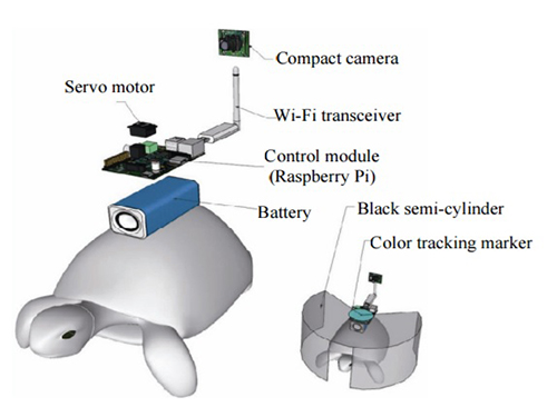
The entire human-turtle setup is as follows: A head-mounted display (HMD) is combined with a BCI to immerse the human user in the turtle’s environment. The human operator wears the BCI-HMD system, while the turtle has a 'cyborg system'—consisting of a camera, Wi-Fi transceiver, computer control module, and battery—all mounted on the turtle’s upper shell. Also included on the turtle’s shell is a black semi-cylinder with a slit, which forms the ‘stimulation device.’ This can be turned ±36 degrees via the BCI.
The entire process works like this: the human operator receives images from the camera mounted on the turtle. These real-time video images allow the human operator to decide where the turtle should move. The human provides thought commands that are recognized by the wearable BCI system as electroencephalography (EEG) signals. The BCI can distinguish between three mental states: left, right, and idle. The left and right commands activate the turtle’s stimulation device via Wi-Fi, turning it so that it obstructs the turtle’s view. This invokes its natural instinct to move toward light and change its direction. Finally, the human acquires updated visual feedback from the camera mounted on the shell and in this way continues to remotely navigate the turtle’s trajectory.
The research demonstrates that the animal guiding scheme via BCI can be used in a variety of environments with turtles moving indoors and outdoors on many different surfaces, like gravel and grass, and tackling a range of obstacles, such as shallow water and trees. This technology could be developed to integrate positioning systems and improved augmented and virtual reality techniques, enabling various applications, including devices for military reconnaissance and surveillance.
***
Reference: “Remote Navigation of Turtle by Controlling Instinct Behavior via Human Brain-computer Interface,” Journal of Bionic Engineering, July 2016 (DOI: 10.1016/S1672-6529(16)60322-0)
Depiction of Cyborg System
A human controller influences the turtle’s escape behavior by sending left and right signals via Wi-Fi to a control system on the back of the turtle.
2017.02.21 View 16997
Controlling Turtle Motion with Human Thought
KAIST researchers have developed a technology that can remotely control an animal’s movement with human thought.
In the 2009 blockbuster “Avatar,” a human remotely controls the body of an alien. It does so by injecting human intelligence into a remotely located, biological body. Although still in the realm of science fiction, researchers are nevertheless developing so-called ‘brain-computer interfaces’ (BCIs) following recent advances in electronics and computing. These technologies can ‘read’ and use human thought to control machines, for example, humanoid robots.
New research has demonstrated the possibility of combining a BCI with a device that transmits information from a computer to a brain, or known as a ‘computer-to-brain interface’ (CBI). The combination of these devices could be used to establish a functional link between the brains of different species. Now, researchers from the Korea Advanced Institute of Science and Technology (KAIST) have developed a human-turtle interaction system in which a signal originating from a human brain can affect where a turtle moves.
Unlike previous research that has tried to control animal movement by applying invasive methods, most notably in insects, Professors Phill-Seung Lee of the Mechanical Engineering Department and Sungho Jo of the Computing School propose a conceptual system that can guide an animal’s moving path by controlling its instinctive escape behavior. They chose a turtle because of its cognitive abilities as well as its ability to distinguish different wavelengths of light. Specifically, turtles can recognize a white light source as an open space and so move toward it. They also show specific avoidance behavior to things that might obstruct their view. Turtles also move toward and away from obstacles in their environment in a predictable manner. It was this instinctive, predictable behavior that the researchers induced using the BCI.
The entire human-turtle setup is as follows: A head-mounted display (HMD) is combined with a BCI to immerse the human user in the turtle’s environment. The human operator wears the BCI-HMD system, while the turtle has a 'cyborg system'—consisting of a camera, Wi-Fi transceiver, computer control module, and battery—all mounted on the turtle’s upper shell. Also included on the turtle’s shell is a black semi-cylinder with a slit, which forms the ‘stimulation device.’ This can be turned ±36 degrees via the BCI.
The entire process works like this: the human operator receives images from the camera mounted on the turtle. These real-time video images allow the human operator to decide where the turtle should move. The human provides thought commands that are recognized by the wearable BCI system as electroencephalography (EEG) signals. The BCI can distinguish between three mental states: left, right, and idle. The left and right commands activate the turtle’s stimulation device via Wi-Fi, turning it so that it obstructs the turtle’s view. This invokes its natural instinct to move toward light and change its direction. Finally, the human acquires updated visual feedback from the camera mounted on the shell and in this way continues to remotely navigate the turtle’s trajectory.
The research demonstrates that the animal guiding scheme via BCI can be used in a variety of environments with turtles moving indoors and outdoors on many different surfaces, like gravel and grass, and tackling a range of obstacles, such as shallow water and trees. This technology could be developed to integrate positioning systems and improved augmented and virtual reality techniques, enabling various applications, including devices for military reconnaissance and surveillance.
***
Reference: “Remote Navigation of Turtle by Controlling Instinct Behavior via Human Brain-computer Interface,” Journal of Bionic Engineering, July 2016 (DOI: 10.1016/S1672-6529(16)60322-0)
Depiction of Cyborg System
A human controller influences the turtle’s escape behavior by sending left and right signals via Wi-Fi to a control system on the back of the turtle.
2017.02.21 View 16997 -
 Making Graphene Using Laser-induced Phase Separation
IBS & KAIST researchers clarify how laser annealing technology can lead to the production of ultrathin nanomaterials
All our smart phones have shiny flat AMOLED (active-matrix organic light-emitting diode) displays. Behind each single pixel of these displays hides at least two silicon transistors which are mass-manufactured using laser annealing technology. While the traditional methods to make the transistors use temperature above 1,000°C, the laser technique reaches the same results at low temperatures even on plastic substrates (melting temperature below 300°C). Interestingly, a similar procedure can be used to generate crystals of graphene. Graphene is a strong and thin nano-material made of carbon, its electric and heat-conductive properties have attracted the attention of scientists worldwide.
Professor Keon Jae Lee of the Materials Science and Engineering Department at KAIST and his research group at the Center for Multidimensional Carbon Materials within the Institute for Basic Science (IBS), as well as Professor Sung-Yool Choi of the Electrical Engineering School at KAIST and his research team discovered graphene synthesis mechanism using laser-induced solid-state phase separation of single-crystal silicon carbide (SiC). This study, available in Nature Communications, clarifies how this laser technology can separate a complex compound (SiC) into its ultrathin elements of carbon and silicon.
Although several fundamental studies presented the effect of excimer lasers in transforming elemental materials like silicon, the laser interaction with more complex compounds like SiC has rarely been studied due to the complexity of compound phase transition and ultra-short processing time.
With high resolution microscope images and molecular dynamic simulations, scientists found that a single-pulse irradiation of xenon chloride excimer laser of 30 nanoseconds melts SiC, leading to the separation of a liquid SiC layer, a disordered carbon layer with graphitic domains (about 2.5 nm thick) on top surface and a polycrystalline silicon layer (about 5 nm) below carbon layer. Giving additional pulses causes the sublimation of the separated silicon, while the disordered carbon layer is transformed into a multilayer graphene.
"This research shows that the laser material interaction technology can be a powerful tool for the next generation of two dimensional nanomaterials," said Professor Lee.
Professor Choi added: "Using laser-induced phase separation of complex compounds, new types of two dimensional materials can be synthesized in the future."
High-resolution transmission electron microscopy shows that after just one laser pulse of 30 nanoseconds, the silicon carbide (SiC) substrate is melted and separates into a carbon and a silicon layer. More pulses cause the carbon layer to organize into graphene and the silicon to leave as gas.
Molecular dynamics simulates the graphene formation mechanism. The carbon layer on the top forms because the laser-induced liquid SiC (SiC (l)) is unstable.
(Press Release by Courtesy of the Institute for Basic Science (IBS))
2016.12.01 View 13307
Making Graphene Using Laser-induced Phase Separation
IBS & KAIST researchers clarify how laser annealing technology can lead to the production of ultrathin nanomaterials
All our smart phones have shiny flat AMOLED (active-matrix organic light-emitting diode) displays. Behind each single pixel of these displays hides at least two silicon transistors which are mass-manufactured using laser annealing technology. While the traditional methods to make the transistors use temperature above 1,000°C, the laser technique reaches the same results at low temperatures even on plastic substrates (melting temperature below 300°C). Interestingly, a similar procedure can be used to generate crystals of graphene. Graphene is a strong and thin nano-material made of carbon, its electric and heat-conductive properties have attracted the attention of scientists worldwide.
Professor Keon Jae Lee of the Materials Science and Engineering Department at KAIST and his research group at the Center for Multidimensional Carbon Materials within the Institute for Basic Science (IBS), as well as Professor Sung-Yool Choi of the Electrical Engineering School at KAIST and his research team discovered graphene synthesis mechanism using laser-induced solid-state phase separation of single-crystal silicon carbide (SiC). This study, available in Nature Communications, clarifies how this laser technology can separate a complex compound (SiC) into its ultrathin elements of carbon and silicon.
Although several fundamental studies presented the effect of excimer lasers in transforming elemental materials like silicon, the laser interaction with more complex compounds like SiC has rarely been studied due to the complexity of compound phase transition and ultra-short processing time.
With high resolution microscope images and molecular dynamic simulations, scientists found that a single-pulse irradiation of xenon chloride excimer laser of 30 nanoseconds melts SiC, leading to the separation of a liquid SiC layer, a disordered carbon layer with graphitic domains (about 2.5 nm thick) on top surface and a polycrystalline silicon layer (about 5 nm) below carbon layer. Giving additional pulses causes the sublimation of the separated silicon, while the disordered carbon layer is transformed into a multilayer graphene.
"This research shows that the laser material interaction technology can be a powerful tool for the next generation of two dimensional nanomaterials," said Professor Lee.
Professor Choi added: "Using laser-induced phase separation of complex compounds, new types of two dimensional materials can be synthesized in the future."
High-resolution transmission electron microscopy shows that after just one laser pulse of 30 nanoseconds, the silicon carbide (SiC) substrate is melted and separates into a carbon and a silicon layer. More pulses cause the carbon layer to organize into graphene and the silicon to leave as gas.
Molecular dynamics simulates the graphene formation mechanism. The carbon layer on the top forms because the laser-induced liquid SiC (SiC (l)) is unstable.
(Press Release by Courtesy of the Institute for Basic Science (IBS))
2016.12.01 View 13307 -
 Graphene-Based Transparent Electrodes for Highly Efficient Flexible OLEDs
A Korean research team developed an ideal electrode structure composed of graphene and layers of titanium dioxide and conducting polymers, resulting in highly flexible and efficient OLEDs.
The arrival of a thin and lightweight computer that even rolls up like a piece of paper will not be in the far distant future. Flexible organic light-emitting diodes (OLEDs), built upon a plastic substrate, have received greater attention lately for their use in next-generation displays that can be bent or rolled while still operating.
A Korean research team led by Professor Seunghyup Yoo from the School of Electrical Engineering, KAIST and Professor Tae-Woo Lee from the Department of Materials Science and Engineering, Pohang University of Science and Technology (POSTECH) has developed highly flexible OLEDs with excellent efficiency by using graphene as a transparent electrode (TE) which is placed in between titanium dioxide (TiO2) and conducting polymer layers. The research results were published online on June 2, 2016 in Nature Communications.
OLEDs are stacked in several ultra-thin layers on glass, foil, or plastic substrates, in which multi-layers of organic compounds are sandwiched between two electrodes (cathode and anode). When voltage is applied across the electrodes, electrons from the cathode and holes (positive charges) from the anode draw toward each other and meet in the emissive layer. OLEDs emit light as an electron recombines with a positive hole, releasing energy in the form of a photon. One of the electrodes in OLEDs is usually transparent, and depending on which electrode is transparent, OLEDs can either emit from the top or bottom.
In conventional bottom-emission OLEDs, an anode is transparent in order for the emitted photons to exit the device through its substrate. Indium-tin-oxide (ITO) is commonly used as a transparent anode because of its high transparency, low sheet resistance, and well-established manufacturing process. However, ITO can potentially be expensive, and moreover, is brittle, being susceptible to bending-induced formation of cracks.
Graphene, a two-dimensional thin layer of carbon atoms tightly bonded together in a hexagonal honeycomb lattice, has recently emerged as an alternative to ITO. With outstanding electrical, physical, and chemical properties, its atomic thinness leading to a high degree of flexibility and transparency makes it an ideal candidate for TEs. Nonetheless, the efficiency of graphene-based OLEDs reported to date has been, at best, about the same level of ITO-based OLEDs.
As a solution, the Korean research team, which further includes Professors Sung-Yool Choi (Electrical Engineering) and Taek-Soo Kim (Mechanical Engineering) of KAIST and their students, proposed a new device architecture that can maximize the efficiency of graphene-based OLEDs. They fabricated a transparent anode in a composite structure in which a TiO2 layer with a high refractive index (high-n) and a hole-injection layer (HIL) of conducting polymers with a low refractive index (low-n) sandwich graphene electrodes. This is an optical design that induces a synergistic collaboration between the high-n and low-n layers to increase the effective reflectance of TEs. As a result, the enhancement of the optical cavity resonance is maximized. The optical cavity resonance is related to the improvement of efficiency and color gamut in OLEDs. At the same time, the loss from surface plasmon polariton (SPP), a major cause for weak photon emissions in OLEDs, is also reduced due to the presence of the low-n conducting polymers.
Under this approach, graphene-based OLEDs exhibit 40.8% of ultrahigh external quantum efficiency (EQE) and 160.3 lm/W of power efficiency, which is unprecedented in those using graphene as a TE. Furthermore, these devices remain intact and operate well even after 1,000 bending cycles at a radius of curvature as small as 2.3 mm. This is a remarkable result for OLEDs containing oxide layers such as TiO2 because oxides are typically brittle and prone to bending-induced fractures even at a relatively low strain. The research team discovered that TiO2 has a crack-deflection toughening mechanism that tends to prevent bending-induced cracks from being formed easily.
Professor Yoo said, “What’s unique and advanced about this technology, compared with previous graphene-based OLEDs, is the synergistic collaboration of high- and low-index layers that enables optical management of both resonance effect and SPP loss, leading to significant enhancement in efficiency, all with little compromise in flexibility.” He added, “Our work was the achievement of collaborative research, transcending the boundaries of different fields, through which we have often found meaningful breakthroughs.”
Professor Lee said, “We expect that our technology will pave the way to develop an OLED light source for highly flexible and wearable displays, or flexible sensors that can be attached to the human body for health monitoring, for instance.”
The research paper is entitled “Synergistic Electrode Architecture for Efficient Graphene-based Flexible Organic Light-emitting Diodes” (DOI. 10.1038/NCOMMS11791). The lead authors are Jae-Ho Lee, a Ph.D. candidate at KAIST; Tae-Hee Han, a Ph.D. researcher at POSTECH; and Min-Ho Park, a Ph.D. candidate at POSTECH.
This study was supported by the Basic Science Research Program of the National Research Foundation of Korea (NRF) through the Center for Advanced Flexible Display (CAFDC) funded by the Ministry of Science, ICT and Future Planning (MSIP); by the Center for Advanced Soft-Electronics funded by the MSIP as a Global Frontier Project; by the Graphene Research Center Program of KAIST; and by grants from the IT R&D Program of the Ministry of Trade, Industry and Energy of Korea (MOTIE).
Figure 1: Application of Graphene-based OLEDs
This picture shows an OLED with the composite structure of TiO2/graphene/conducting polymer electrode in operation. The OLED exhibits 40.8% of ultrahigh external quantum efficiency (EQE) and 160.3 lm/W of power efficiency. The device prepared on a plastic substrate shown in the right remains intact and operates well even after 1,000 bending cycles at a radius of curvature as small as 2.3 mm.
Figure 2: Schematic Device Structure of Graphene-based OLEDs
This picture shows the new architecture to develop highly flexible OLEDs with excellent efficiency by using graphene as a transparent electrode (TE).
2016.06.07 View 16155
Graphene-Based Transparent Electrodes for Highly Efficient Flexible OLEDs
A Korean research team developed an ideal electrode structure composed of graphene and layers of titanium dioxide and conducting polymers, resulting in highly flexible and efficient OLEDs.
The arrival of a thin and lightweight computer that even rolls up like a piece of paper will not be in the far distant future. Flexible organic light-emitting diodes (OLEDs), built upon a plastic substrate, have received greater attention lately for their use in next-generation displays that can be bent or rolled while still operating.
A Korean research team led by Professor Seunghyup Yoo from the School of Electrical Engineering, KAIST and Professor Tae-Woo Lee from the Department of Materials Science and Engineering, Pohang University of Science and Technology (POSTECH) has developed highly flexible OLEDs with excellent efficiency by using graphene as a transparent electrode (TE) which is placed in between titanium dioxide (TiO2) and conducting polymer layers. The research results were published online on June 2, 2016 in Nature Communications.
OLEDs are stacked in several ultra-thin layers on glass, foil, or plastic substrates, in which multi-layers of organic compounds are sandwiched between two electrodes (cathode and anode). When voltage is applied across the electrodes, electrons from the cathode and holes (positive charges) from the anode draw toward each other and meet in the emissive layer. OLEDs emit light as an electron recombines with a positive hole, releasing energy in the form of a photon. One of the electrodes in OLEDs is usually transparent, and depending on which electrode is transparent, OLEDs can either emit from the top or bottom.
In conventional bottom-emission OLEDs, an anode is transparent in order for the emitted photons to exit the device through its substrate. Indium-tin-oxide (ITO) is commonly used as a transparent anode because of its high transparency, low sheet resistance, and well-established manufacturing process. However, ITO can potentially be expensive, and moreover, is brittle, being susceptible to bending-induced formation of cracks.
Graphene, a two-dimensional thin layer of carbon atoms tightly bonded together in a hexagonal honeycomb lattice, has recently emerged as an alternative to ITO. With outstanding electrical, physical, and chemical properties, its atomic thinness leading to a high degree of flexibility and transparency makes it an ideal candidate for TEs. Nonetheless, the efficiency of graphene-based OLEDs reported to date has been, at best, about the same level of ITO-based OLEDs.
As a solution, the Korean research team, which further includes Professors Sung-Yool Choi (Electrical Engineering) and Taek-Soo Kim (Mechanical Engineering) of KAIST and their students, proposed a new device architecture that can maximize the efficiency of graphene-based OLEDs. They fabricated a transparent anode in a composite structure in which a TiO2 layer with a high refractive index (high-n) and a hole-injection layer (HIL) of conducting polymers with a low refractive index (low-n) sandwich graphene electrodes. This is an optical design that induces a synergistic collaboration between the high-n and low-n layers to increase the effective reflectance of TEs. As a result, the enhancement of the optical cavity resonance is maximized. The optical cavity resonance is related to the improvement of efficiency and color gamut in OLEDs. At the same time, the loss from surface plasmon polariton (SPP), a major cause for weak photon emissions in OLEDs, is also reduced due to the presence of the low-n conducting polymers.
Under this approach, graphene-based OLEDs exhibit 40.8% of ultrahigh external quantum efficiency (EQE) and 160.3 lm/W of power efficiency, which is unprecedented in those using graphene as a TE. Furthermore, these devices remain intact and operate well even after 1,000 bending cycles at a radius of curvature as small as 2.3 mm. This is a remarkable result for OLEDs containing oxide layers such as TiO2 because oxides are typically brittle and prone to bending-induced fractures even at a relatively low strain. The research team discovered that TiO2 has a crack-deflection toughening mechanism that tends to prevent bending-induced cracks from being formed easily.
Professor Yoo said, “What’s unique and advanced about this technology, compared with previous graphene-based OLEDs, is the synergistic collaboration of high- and low-index layers that enables optical management of both resonance effect and SPP loss, leading to significant enhancement in efficiency, all with little compromise in flexibility.” He added, “Our work was the achievement of collaborative research, transcending the boundaries of different fields, through which we have often found meaningful breakthroughs.”
Professor Lee said, “We expect that our technology will pave the way to develop an OLED light source for highly flexible and wearable displays, or flexible sensors that can be attached to the human body for health monitoring, for instance.”
The research paper is entitled “Synergistic Electrode Architecture for Efficient Graphene-based Flexible Organic Light-emitting Diodes” (DOI. 10.1038/NCOMMS11791). The lead authors are Jae-Ho Lee, a Ph.D. candidate at KAIST; Tae-Hee Han, a Ph.D. researcher at POSTECH; and Min-Ho Park, a Ph.D. candidate at POSTECH.
This study was supported by the Basic Science Research Program of the National Research Foundation of Korea (NRF) through the Center for Advanced Flexible Display (CAFDC) funded by the Ministry of Science, ICT and Future Planning (MSIP); by the Center for Advanced Soft-Electronics funded by the MSIP as a Global Frontier Project; by the Graphene Research Center Program of KAIST; and by grants from the IT R&D Program of the Ministry of Trade, Industry and Energy of Korea (MOTIE).
Figure 1: Application of Graphene-based OLEDs
This picture shows an OLED with the composite structure of TiO2/graphene/conducting polymer electrode in operation. The OLED exhibits 40.8% of ultrahigh external quantum efficiency (EQE) and 160.3 lm/W of power efficiency. The device prepared on a plastic substrate shown in the right remains intact and operates well even after 1,000 bending cycles at a radius of curvature as small as 2.3 mm.
Figure 2: Schematic Device Structure of Graphene-based OLEDs
This picture shows the new architecture to develop highly flexible OLEDs with excellent efficiency by using graphene as a transparent electrode (TE).
2016.06.07 View 16155 -
 Professor Keon-Jae Lee Lectures at IEDM and ISSCC Forums
Professor Keon-Jae Lee of KAIST’s Materials Science and Engineering Department delivered a speech at the 2015 Institute of Electrical and Electronics Engineers (IEEE) International Electron Devices Meeting (IEDM) held on December 7-9, 2015 in Washington, D.C.
He will also present a speech at the 2016 International Solid-State Circuits Conference scheduled on January 31-February 4, 2016 in San Francisco, California.
Both professional gatherings are considered the world’s most renowned forums in electronic devices and semiconductor technology. It is rare for a Korean researcher to be invited to speak at these global conferences.
Professor Lee was recognized for his research on flexible NAND chips. The Korea Times, an English language daily newspaper in Korea, reported on his participation in the forums and his recent work. An excerpt of the article follows below:
“KAIST Professor to Lecture at Renowned Tech Forums”
By Lee Min-hyung, The Korea Times, November 26, 2015
Recently he has focused on delivering technologies for producing flexible materials that can be applied to everyday life. The flexible NAND flash memory chips are expected to be widely used for developing flexible handsets. His latest research also includes flexible light-emitting diodes (LED) for implantable biomedical applications.
Lee is currently running a special laboratory focused on developing new flexible nano-materials. The research group is working to develop what it calls “self-powered flexible electronic systems” using nanomaterials and electronic technology.
Lee’s achievement with flexible NAND chips was published in the October edition of Nano Letters, the renowned U.S.-based scientific journal.
He said that flexible memory chips will be used to develop wearable computers that can be installed anywhere.
2015.11.26 View 14903
Professor Keon-Jae Lee Lectures at IEDM and ISSCC Forums
Professor Keon-Jae Lee of KAIST’s Materials Science and Engineering Department delivered a speech at the 2015 Institute of Electrical and Electronics Engineers (IEEE) International Electron Devices Meeting (IEDM) held on December 7-9, 2015 in Washington, D.C.
He will also present a speech at the 2016 International Solid-State Circuits Conference scheduled on January 31-February 4, 2016 in San Francisco, California.
Both professional gatherings are considered the world’s most renowned forums in electronic devices and semiconductor technology. It is rare for a Korean researcher to be invited to speak at these global conferences.
Professor Lee was recognized for his research on flexible NAND chips. The Korea Times, an English language daily newspaper in Korea, reported on his participation in the forums and his recent work. An excerpt of the article follows below:
“KAIST Professor to Lecture at Renowned Tech Forums”
By Lee Min-hyung, The Korea Times, November 26, 2015
Recently he has focused on delivering technologies for producing flexible materials that can be applied to everyday life. The flexible NAND flash memory chips are expected to be widely used for developing flexible handsets. His latest research also includes flexible light-emitting diodes (LED) for implantable biomedical applications.
Lee is currently running a special laboratory focused on developing new flexible nano-materials. The research group is working to develop what it calls “self-powered flexible electronic systems” using nanomaterials and electronic technology.
Lee’s achievement with flexible NAND chips was published in the October edition of Nano Letters, the renowned U.S.-based scientific journal.
He said that flexible memory chips will be used to develop wearable computers that can be installed anywhere.
2015.11.26 View 14903 -
 Open KAIST 2015
KAIST’s research environment and its most recent achievements were open to the public.
KAIST hosted “Open KAIST 2015” over two days from November 5-6, 2015 in which its 17 departments and three research centers were open to the public. The event is one of the largest events that KAIST holds, which permits such public viewings of its facilities. It is the eighth time it has taken place.
During this event, the departments and centers offered 64 programs including laboratory tours, research achievement exhibitions, department introductions, and special lectures.
The “Motion Capture System”of Professor Jun-Yong Noh’s lab (Graduate School of Culture Technology) drew particular attention.
The “Motion Capture System” expresses human and animal motion in three-dimensional (3D) space using infrared cameras and optic markers, which can then be applied to various industries such as movies, games, and animation. During the program, researchers themselves demonstrated the recording of the movement and its conversion into 3D characters.
Professor Yong-Hoon Cho’s laboratory introduced the scientific mechanism behind the Light Emitting Diode (LED) as well as its manufacturing process under the topic:“A to Z of LED Production.” The reserachers explained that how green LED is much more efficient compared to previous light sources and presented applications that how it is widely used in everyday life in smart phones, electronic displays, and other mobile gadgets.
Professor Jun-tani of the Department of Electronic and Electrical Engineering introduced “Humanoid Robot Nao’s Imitation of Human Motions.” Nao is an autonomous, programmable humanoid robot developed by a French robotics company based in Paris. Nao has an artificial neural circuit, which is the functional equivalent of a human brain, and can thus mimic the subject’s motions through learning.
In addition, Professor Hyo-Choong Bang (Department of Aerospace Engineering) in his lecture on “Unmanned Vehicle Research and Nano Satellites” and Professor Hyun Myung (Department of Civil and Environmental Engineering) on his lecture on “Future Civilization Robot System: the Jellyfish Elimination Robotic Swarm and the Wall-Climbing Drone” provided information on the progress of their respective research.
KAIST also displayed its most recent research achievements. A lecture on “Information Technology Convergence” offered a showroom for “Dr. M,” which is a mobile healthcare platform. Dr. M is a mobile healthcare system that collects and analyzes biosignals via a smart sensor attached to the human body that shows around 20 advanced technologies.
The Satellite Technology Research Center introduced the public to its “Get to Know Satellites” program on Korea’s first satellite “Our Star 1” in addition to showing the satellite assembly room and the satellite communication center.
Special lectures were also held for visitors. Professor Min-Hyuk Kim and Hye-Yeon Oh of the School of Computing talked about “Computer Graphics and Advanced Video Technology” and “Man and the Computer,” respectively, from the perspective of non-experts.
Another interesting feature was the “Wearable Computer Competition” in which college students held fashion shows with computers attached to their clothes.
Professor Jung Kwon Lee, the Dean of the College of Engineering, who led this event, said that “the Open KAIST, which is being held for the eighth time this year, is an excellent opportunity for the general public to experience KAIST’s research environment.” He hoped this could motivate young adults to widen their spectrum of scientific knowledge and raise affection for science.
2015.11.13 View 13632
Open KAIST 2015
KAIST’s research environment and its most recent achievements were open to the public.
KAIST hosted “Open KAIST 2015” over two days from November 5-6, 2015 in which its 17 departments and three research centers were open to the public. The event is one of the largest events that KAIST holds, which permits such public viewings of its facilities. It is the eighth time it has taken place.
During this event, the departments and centers offered 64 programs including laboratory tours, research achievement exhibitions, department introductions, and special lectures.
The “Motion Capture System”of Professor Jun-Yong Noh’s lab (Graduate School of Culture Technology) drew particular attention.
The “Motion Capture System” expresses human and animal motion in three-dimensional (3D) space using infrared cameras and optic markers, which can then be applied to various industries such as movies, games, and animation. During the program, researchers themselves demonstrated the recording of the movement and its conversion into 3D characters.
Professor Yong-Hoon Cho’s laboratory introduced the scientific mechanism behind the Light Emitting Diode (LED) as well as its manufacturing process under the topic:“A to Z of LED Production.” The reserachers explained that how green LED is much more efficient compared to previous light sources and presented applications that how it is widely used in everyday life in smart phones, electronic displays, and other mobile gadgets.
Professor Jun-tani of the Department of Electronic and Electrical Engineering introduced “Humanoid Robot Nao’s Imitation of Human Motions.” Nao is an autonomous, programmable humanoid robot developed by a French robotics company based in Paris. Nao has an artificial neural circuit, which is the functional equivalent of a human brain, and can thus mimic the subject’s motions through learning.
In addition, Professor Hyo-Choong Bang (Department of Aerospace Engineering) in his lecture on “Unmanned Vehicle Research and Nano Satellites” and Professor Hyun Myung (Department of Civil and Environmental Engineering) on his lecture on “Future Civilization Robot System: the Jellyfish Elimination Robotic Swarm and the Wall-Climbing Drone” provided information on the progress of their respective research.
KAIST also displayed its most recent research achievements. A lecture on “Information Technology Convergence” offered a showroom for “Dr. M,” which is a mobile healthcare platform. Dr. M is a mobile healthcare system that collects and analyzes biosignals via a smart sensor attached to the human body that shows around 20 advanced technologies.
The Satellite Technology Research Center introduced the public to its “Get to Know Satellites” program on Korea’s first satellite “Our Star 1” in addition to showing the satellite assembly room and the satellite communication center.
Special lectures were also held for visitors. Professor Min-Hyuk Kim and Hye-Yeon Oh of the School of Computing talked about “Computer Graphics and Advanced Video Technology” and “Man and the Computer,” respectively, from the perspective of non-experts.
Another interesting feature was the “Wearable Computer Competition” in which college students held fashion shows with computers attached to their clothes.
Professor Jung Kwon Lee, the Dean of the College of Engineering, who led this event, said that “the Open KAIST, which is being held for the eighth time this year, is an excellent opportunity for the general public to experience KAIST’s research environment.” He hoped this could motivate young adults to widen their spectrum of scientific knowledge and raise affection for science.
2015.11.13 View 13632 -
 Dr. Se-Jung Kim Receives the Grand Prize at the International Photo and Image Contest on Light
Dr. Se-Jung Kim of the Physics Department at KAIST received the Grand Prize at the 2015 Photo and Image Contest of the International Year of Light and Light-based Technologies.
The United Nations has designated the year 2015 as the International Year of Light and Light-based Technologies.
The Optical Society of Korea celebrated the UN’s designation by hosting an international photo and image contest on the theme of light and optics related technology.
Dr. Kim presented a photo of images taken from a liquid crystal, which was entitled “A Micro Pinwheel.” She took pictures of liquid crystal images with a polarizing microscope and then colored the pictures. The liquid crystal has self-assembled circle domain structures, and each domain can form vortex optics. Her adviser for the project is Professor Yong-Hoon Cho of the Physics Department.
Her work was exhibited during the annual conference of the Optical Society of Korea, which was held on July 13-15, 2015 at Gyeong-Ju Hwabaek International Convention Center. It will also be exhibited at the National Science Museum in Gwacheon and the Kim Dae-Jung Convention Center in Gwangju.
Picture: A Micro Pinwheel
2015.07.31 View 13211
Dr. Se-Jung Kim Receives the Grand Prize at the International Photo and Image Contest on Light
Dr. Se-Jung Kim of the Physics Department at KAIST received the Grand Prize at the 2015 Photo and Image Contest of the International Year of Light and Light-based Technologies.
The United Nations has designated the year 2015 as the International Year of Light and Light-based Technologies.
The Optical Society of Korea celebrated the UN’s designation by hosting an international photo and image contest on the theme of light and optics related technology.
Dr. Kim presented a photo of images taken from a liquid crystal, which was entitled “A Micro Pinwheel.” She took pictures of liquid crystal images with a polarizing microscope and then colored the pictures. The liquid crystal has self-assembled circle domain structures, and each domain can form vortex optics. Her adviser for the project is Professor Yong-Hoon Cho of the Physics Department.
Her work was exhibited during the annual conference of the Optical Society of Korea, which was held on July 13-15, 2015 at Gyeong-Ju Hwabaek International Convention Center. It will also be exhibited at the National Science Museum in Gwacheon and the Kim Dae-Jung Convention Center in Gwangju.
Picture: A Micro Pinwheel
2015.07.31 View 13211 -
 Professor Jae Kyu Lee Appointed the President of Association for Information Systems
Chair Professor Jae Kyu Lee of KAIST’s College of Business was appointed the President of Association for Information Systems (AIS) on July 1, 2015. Professor Lee will serve a one-year term, which will end in June 2016. With four thousand members researching information systems from 90 different nations, AIS is the largest academic society in the fields of information system and business process engineering.
Professor Lee has proposed his idea of “the Bright Internet” as the official vision of AIS. Employing this vision, AIS will create technology and systems, as well as sponsor international cooperation to solve fundamental issues of the Internet including concerns over hacking and cyber-related crimes.
The extent of damage from cyber-related crimes grows each year. Every day, 56 billion junk emails are sent to computers which are hacked and become “zombie” computers. The social cost of such crimes is estimated to be 400 billion US dollars annually.
Based on "the Bright Internet," AIS will build a preventative Internet security system by adopting ground rules that make attackers responsible for the damages from such crimes. The system will also modify technology and other systems to minimize privacy infringement while maintaining security. Finally, the Bright Internet proposes to adopt an international standard for this security system through collaboration with the International Telecommunications Union (ITU).
Professor Lee said, “The vision of the Bright Internet started from an awareness that we needed to resolve issues such as Internet addiction, indiscriminate media exposure, and verbal violence. This vision developed by the experts from all around the world will not only bring a revolution of a reliable Internet platform to a global scale but also reshape the Korean Internet platform.”
2015.07.02 View 9719
Professor Jae Kyu Lee Appointed the President of Association for Information Systems
Chair Professor Jae Kyu Lee of KAIST’s College of Business was appointed the President of Association for Information Systems (AIS) on July 1, 2015. Professor Lee will serve a one-year term, which will end in June 2016. With four thousand members researching information systems from 90 different nations, AIS is the largest academic society in the fields of information system and business process engineering.
Professor Lee has proposed his idea of “the Bright Internet” as the official vision of AIS. Employing this vision, AIS will create technology and systems, as well as sponsor international cooperation to solve fundamental issues of the Internet including concerns over hacking and cyber-related crimes.
The extent of damage from cyber-related crimes grows each year. Every day, 56 billion junk emails are sent to computers which are hacked and become “zombie” computers. The social cost of such crimes is estimated to be 400 billion US dollars annually.
Based on "the Bright Internet," AIS will build a preventative Internet security system by adopting ground rules that make attackers responsible for the damages from such crimes. The system will also modify technology and other systems to minimize privacy infringement while maintaining security. Finally, the Bright Internet proposes to adopt an international standard for this security system through collaboration with the International Telecommunications Union (ITU).
Professor Lee said, “The vision of the Bright Internet started from an awareness that we needed to resolve issues such as Internet addiction, indiscriminate media exposure, and verbal violence. This vision developed by the experts from all around the world will not only bring a revolution of a reliable Internet platform to a global scale but also reshape the Korean Internet platform.”
2015.07.02 View 9719 -
 The College of Information Science & Technology names its Alumnus of the Year 2014
The College of Information Science & Technology (CIST), KAIST, selected Tae-Kyung Yoo, the Chief Executive Officer of Lumens, Inc., a Korean company producing semiconductors and light emitting diodes (LEDs), as its Alumnus of the Year 2014.
The award ceremony took place on September 19, 2014 at the KAIST Institute with the participation of the university’s senior management and students.
Mr. Yoo was recognized for his pioneering work to develop the LED industry in Korea as the next-generation growth engine for the nation’s economy.
After the ceremony, he gave a talk entitled “The Past and Future of the LED Industry: Its Important Role in the Change of Korean Industry.”
The CIST created the Alumnus of the Year 2014 award, for the first time this year, to appreciate its alumni’s contribution to the advancement of the industrial and academic sectors of Korean information science and technology, and it will continue presenting the award from this year onwards.
2014.09.22 View 8451
The College of Information Science & Technology names its Alumnus of the Year 2014
The College of Information Science & Technology (CIST), KAIST, selected Tae-Kyung Yoo, the Chief Executive Officer of Lumens, Inc., a Korean company producing semiconductors and light emitting diodes (LEDs), as its Alumnus of the Year 2014.
The award ceremony took place on September 19, 2014 at the KAIST Institute with the participation of the university’s senior management and students.
Mr. Yoo was recognized for his pioneering work to develop the LED industry in Korea as the next-generation growth engine for the nation’s economy.
After the ceremony, he gave a talk entitled “The Past and Future of the LED Industry: Its Important Role in the Change of Korean Industry.”
The CIST created the Alumnus of the Year 2014 award, for the first time this year, to appreciate its alumni’s contribution to the advancement of the industrial and academic sectors of Korean information science and technology, and it will continue presenting the award from this year onwards.
2014.09.22 View 8451 -
 Kinetic Lighting, Dlight, Dominates World Renowned Design Awards
Professor Sang-Min Bae
“D’light,” a lamp that transforms its lampshade shape, developed by a team led by KAIST Department of Industrial Design’s Professor Sang-Min Bae, won Japan’s Good Design Awards on October the 2nd, soon after winning the internationally renowned 2013 International Design Excellence Awards (IDEA) in August.
IDEA, sponsored by the Industrial Design Society of America (IDSA) and BusinessWeek, awards the best work from over 6,000 exhibits from 50 countries. Japan’s Good Design Awards, founded by the Japan Institute of Design Promotion (JDP) in 1957, is the most prestigious and one of the World’s four major design awards.
“D’light” combines “donative” and “light.” Its meaning originates from the meaning of “delight” which means “giving great joy.” The shape and the brightness of the lamp can be transformed by turning the end of the heart-shaped lampshade. The team states that the lamp carries a figurative meaning of generous hearts lighting the neglected of the world by designing the lamp to be the brightest when it takes the shape of a heart. D’light developed as the 5th product of “the Nanum” project that started in 2006. Professor Bae first participated in the project in developing the 2nd product, “Cross Cube” in 2007. The he designed and launched the environmentally friendly humidifier “Lovepot” in 2008 and interactive tumbler “Hearty” in 2009.
The “Nanum” project aims to develop innovative products for charity to create a humane social circulatory system. The project, led by the international relief and development organisation, World Vision and KAIST’s ID+IM laboratory run by Professor Bae, donates all profits to educate the children of low-income families. The project raised a total of 1.7 billion Korean won from 2007 this year to provide scholarships to 240 children in need.
Professor Bae’s team has undertaken seed and “Nanum” projects with the theme of philanthropy design helping people in need by creating innovative designs. The project has produced four excellent and authentic products which received 44 world renowned design awards.
Professor Bae said, “’The Nanum’ project consists of planning, designing, producing and selling for charity and donates all profit to children in need through education and scholarship.” He continued, “The consumers can purchase products that are aesthetically pleasing and convenient as well as gaining an opportunity to donate to children in need.”
Figure1 Kinetic lighting D’light
Figure 2. Characteristics of “Nanum” D’light
The shape of the lampshade can be transformed. The lamp sheds the brightest light when it takes the shape of a heart, hence showing the figurative meaning of brightening the neglected parts of the world with generous hearts.
Figure 3. Detailed Images of D’light
2013.11.11 View 12155
Kinetic Lighting, Dlight, Dominates World Renowned Design Awards
Professor Sang-Min Bae
“D’light,” a lamp that transforms its lampshade shape, developed by a team led by KAIST Department of Industrial Design’s Professor Sang-Min Bae, won Japan’s Good Design Awards on October the 2nd, soon after winning the internationally renowned 2013 International Design Excellence Awards (IDEA) in August.
IDEA, sponsored by the Industrial Design Society of America (IDSA) and BusinessWeek, awards the best work from over 6,000 exhibits from 50 countries. Japan’s Good Design Awards, founded by the Japan Institute of Design Promotion (JDP) in 1957, is the most prestigious and one of the World’s four major design awards.
“D’light” combines “donative” and “light.” Its meaning originates from the meaning of “delight” which means “giving great joy.” The shape and the brightness of the lamp can be transformed by turning the end of the heart-shaped lampshade. The team states that the lamp carries a figurative meaning of generous hearts lighting the neglected of the world by designing the lamp to be the brightest when it takes the shape of a heart. D’light developed as the 5th product of “the Nanum” project that started in 2006. Professor Bae first participated in the project in developing the 2nd product, “Cross Cube” in 2007. The he designed and launched the environmentally friendly humidifier “Lovepot” in 2008 and interactive tumbler “Hearty” in 2009.
The “Nanum” project aims to develop innovative products for charity to create a humane social circulatory system. The project, led by the international relief and development organisation, World Vision and KAIST’s ID+IM laboratory run by Professor Bae, donates all profits to educate the children of low-income families. The project raised a total of 1.7 billion Korean won from 2007 this year to provide scholarships to 240 children in need.
Professor Bae’s team has undertaken seed and “Nanum” projects with the theme of philanthropy design helping people in need by creating innovative designs. The project has produced four excellent and authentic products which received 44 world renowned design awards.
Professor Bae said, “’The Nanum’ project consists of planning, designing, producing and selling for charity and donates all profit to children in need through education and scholarship.” He continued, “The consumers can purchase products that are aesthetically pleasing and convenient as well as gaining an opportunity to donate to children in need.”
Figure1 Kinetic lighting D’light
Figure 2. Characteristics of “Nanum” D’light
The shape of the lampshade can be transformed. The lamp sheds the brightest light when it takes the shape of a heart, hence showing the figurative meaning of brightening the neglected parts of the world with generous hearts.
Figure 3. Detailed Images of D’light
2013.11.11 View 12155 -
 Transparent Glass Wall as a Touch Game Media
Professor Woo-hoon Lee
- Selected as the “Highlight” at SIGGRAPH emerging technology conference
- “An excellent example of the transparent display panel in everyday life”
A joint research team led by KAIST Industrial Design Department’s Prof. Woo-hoon Lee and Computer Sciences Prof. Ki-hyuk Lee has developed a brand new concept game media “TransWall”, which utilizes both sides of the glass wall as the touch medium.
TransWall has been chosen as the “highlight” of 2013 SIGGRAPH emerging technology conference. SIGGRAPH is a world-renowned conference in the area of computer graphics and interaction technique, last held 21st-25th July at Anaheim, in the United States.
It all started with the thought, wouldn’t it be possible to turn the glass walls surrounding us into a medium for entertainment and communication?
TransWall utilizes holographic screen film inserted between two glass sheets with a multi-touch function, onto which the image can be projected using the beam projector from both sides. Furthermore, an additional Surface Transducer attached to the glass can deliver the sound and vibration.
What seemed as an ordinary glass wall has been transformed into a multi-sensory media that can transmit and receive visual, auditory and tactile information.
TransWall can be implemented at public places such as theme parks, large shopping malls and subway stations, providing the citizens with a new form of entertainment. This touch-interaction method can also be applied to developing a variety of cultural contents in the future.
Professor Lee said, “TransWall shows an example of near-future where touch-interaction method can be utilized with the soon-to-be commercialized transparent display panel in everyday lives.”
TransWall Introduction video (https://vimeo.com/70391422)
TransWall at SIGGRAPH 2013 Display (https://vimeo.com/71718874)
Picture 1. Both sides of the glass wall can be used as a touch platform for various medias, including games.
Picture 2. TransWall attracts the interests of the audience at SIGGRAPH emerging technology.
Picture 3. Structure of TransWall
Picture 4. Photo of TransWall from side
2013.09.19 View 11993
Transparent Glass Wall as a Touch Game Media
Professor Woo-hoon Lee
- Selected as the “Highlight” at SIGGRAPH emerging technology conference
- “An excellent example of the transparent display panel in everyday life”
A joint research team led by KAIST Industrial Design Department’s Prof. Woo-hoon Lee and Computer Sciences Prof. Ki-hyuk Lee has developed a brand new concept game media “TransWall”, which utilizes both sides of the glass wall as the touch medium.
TransWall has been chosen as the “highlight” of 2013 SIGGRAPH emerging technology conference. SIGGRAPH is a world-renowned conference in the area of computer graphics and interaction technique, last held 21st-25th July at Anaheim, in the United States.
It all started with the thought, wouldn’t it be possible to turn the glass walls surrounding us into a medium for entertainment and communication?
TransWall utilizes holographic screen film inserted between two glass sheets with a multi-touch function, onto which the image can be projected using the beam projector from both sides. Furthermore, an additional Surface Transducer attached to the glass can deliver the sound and vibration.
What seemed as an ordinary glass wall has been transformed into a multi-sensory media that can transmit and receive visual, auditory and tactile information.
TransWall can be implemented at public places such as theme parks, large shopping malls and subway stations, providing the citizens with a new form of entertainment. This touch-interaction method can also be applied to developing a variety of cultural contents in the future.
Professor Lee said, “TransWall shows an example of near-future where touch-interaction method can be utilized with the soon-to-be commercialized transparent display panel in everyday lives.”
TransWall Introduction video (https://vimeo.com/70391422)
TransWall at SIGGRAPH 2013 Display (https://vimeo.com/71718874)
Picture 1. Both sides of the glass wall can be used as a touch platform for various medias, including games.
Picture 2. TransWall attracts the interests of the audience at SIGGRAPH emerging technology.
Picture 3. Structure of TransWall
Picture 4. Photo of TransWall from side
2013.09.19 View 11993 -
2012 Intellectual Property Rights Award Ceremony Held
The 2012 Intellectual Property Rights Award Ceremony was held at Seoul KAIST Campus.
Recipients of the award included former congressmen Kim Young Sun and Lee Jeong Hyuk, and Kim Boo Kyung researcher at Electronics and Telecommunications Research Institute also representing Vooz Ltd. that created the character POOCA.
The Intellectual Property Rights Award is given to an individual or a group that succeeded in utilizing, protecting, creating, and establishment of its foundation including patent, copyright, and brand. Intellectual Property Rights is viewed as of importance for future national competitiveness.
The Award is organized by the Korea Patent Attorneys Association, the Korea Association of Intellectual Property Services, and KAIST and are respectively core institutions in the training of Intellectual Property Rights Experts and the creation, utilization, and the protection of intellectual property.
In addition the Award is also co-organized by the KAIST Graduate School of Intellectual Property Rights (established in cooperation with KAIST and the Korean Intellectual Property Office) and the total 20 million Won of prize money is funded by Korea Institute of Intellectual Strategy and Kim Ok Lan Foundation.
The Award Ceremony was held with a special lecture by the recipients.
It was stressed that the evaluation process was carried out with that the decision is a silent message to the society and is also a type of market signal.
Director Ko Gi Seok (Presidential Council on Intellectual Property) revealed that the candidates’ impact on the strength of national intellectual property rights was thoroughly scrutinized.
In the criteria of Creation of Intellectual Property, ETRI received the award in recognition of the institution’s successful patenting and commercializing of products of Korean R&D.
ETRI created a total of 251 International Patents in cooperation with ITU, ISO, IEE, etc. and also participated in a total of 9 International Standard Patent Pool, showing its active Intellectual Property management.
Such efforts ranked ETRI 1st in the United States Patent Evaluation performed by the US Patent Board in 2011 out of 237 institutions.
In addition Recipient of the Intellectual Property Utilization criteria, VOOZ ltd.’s Kim Boo Kyung promised the free use of their character POOCA in ETRI’s automated Korean-English translator. Researcher Kim Boo Kyung was rewarded with the award in recognition of his contribution to the domestic economy and realization of the commercialization of a copy right through licensing.
Former congressman Kim Young Son received an Award in the Foundation criteria in recognition of his efforts in the establishment of the Presidential Council on Intellectual Property and the Basic Blueprints for the Intellectual Property Law.
Former congressman Lee Jeong Hyuk received the same award in recognition of standardization and streamlining Intellectual Property Rights Policies. His realization and pursuit of the establishment of a balanced growth based on law for the competitiveness of businesses was the driving force behind his accomplishments.
2012.10.16 View 13931
-
Op-Ed by MIT President, Manufacturing a Recovery, New York Times, August 29, 2011
New York Times carried an opinion piece of MIT President, Susan Hockfield. Dr. Hockfield put emphasis on the importance of recovering manufacturing to revive the US economy and suggested investments in the development of high technology and “tight integration of design production” through “networks of innovation, lab research to new production processes, and business models.” For the op-ed piece, please go to
http://www.nytimes.com/2011/08/30/opinion/manufacturing-a-recovery.html?_r=2.
2011.08.31 View 12072