Chem
-
 Distinguished Professor Sukbok Chang Donates His Prize Money
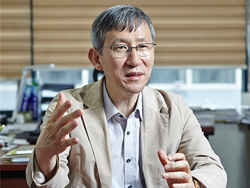
The honoree of the 2019 Korea Best Scientist and Technologist Award, Distinguished Professor Sukbok Chang donated his prize money of one hundred million KRW to the Chemistry Department Scholarship Fund and the Lyu Keun-Chul Sports Complex Management Fund during a donation ceremony last week.
Professor Chang won the award last month in recognition of his pioneering achievements and lifetime contributions to the development of carbon-hydrogen activation strategies, especially for carbon-carbon, carbon-nitrogen, and carbon-oxygen formations. Professor Chang, a world renowned chemist, has been recognized for his highly selective catalytic systems, allowing the controlled defunctionalization of bio-derived platform substrates under mild conditions and opening a new avenue for the utilization of biomass-derived platform chemicals.
“All my achievements are the results of my students’ hard work and dedication. I feel very fortunate to have such talented team members. I want to express my sincere gratitude for such a great research environment that we have worked together in so far,” said Professor Chang at the ceremony.
KAIST President Sung-Chul Shin said, “Not only will Professor Chang’s donation make a significant contribution to the Department of Chemistry, but also to the improvement of the Lyu Keun-Chul Sports Complex’s management, which directly links to the health and welfare of the KAIST community.”
Professor Chang currently holds the position of distinguished professor at KAIST and director of the Center for Catalytic Hydrocarbon Functionalizations in the Institute for Basic Science (IBS). He previously received the Kyung-Ahm Academic Award in 2013 and the Korea Toray Science Award in 2018. All these prize money also went to the school.
(END)
2019.08.26 View 8981
Distinguished Professor Sukbok Chang Donates His Prize Money
The honoree of the 2019 Korea Best Scientist and Technologist Award, Distinguished Professor Sukbok Chang donated his prize money of one hundred million KRW to the Chemistry Department Scholarship Fund and the Lyu Keun-Chul Sports Complex Management Fund during a donation ceremony last week.
Professor Chang won the award last month in recognition of his pioneering achievements and lifetime contributions to the development of carbon-hydrogen activation strategies, especially for carbon-carbon, carbon-nitrogen, and carbon-oxygen formations. Professor Chang, a world renowned chemist, has been recognized for his highly selective catalytic systems, allowing the controlled defunctionalization of bio-derived platform substrates under mild conditions and opening a new avenue for the utilization of biomass-derived platform chemicals.
“All my achievements are the results of my students’ hard work and dedication. I feel very fortunate to have such talented team members. I want to express my sincere gratitude for such a great research environment that we have worked together in so far,” said Professor Chang at the ceremony.
KAIST President Sung-Chul Shin said, “Not only will Professor Chang’s donation make a significant contribution to the Department of Chemistry, but also to the improvement of the Lyu Keun-Chul Sports Complex’s management, which directly links to the health and welfare of the KAIST community.”
Professor Chang currently holds the position of distinguished professor at KAIST and director of the Center for Catalytic Hydrocarbon Functionalizations in the Institute for Basic Science (IBS). He previously received the Kyung-Ahm Academic Award in 2013 and the Korea Toray Science Award in 2018. All these prize money also went to the school.
(END)
2019.08.26 View 8981 -
 Enhanced Natural Gas Storage to Help Reduce Global Warming
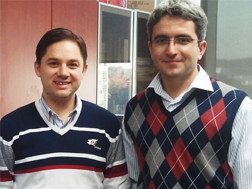
< Professor Atilhan (left) and Professor Yavuz (right) >
Researchers have designed plastic-based materials that can store natural gas more effectively. These new materials can not only make large-scale, cost-effective, and safe natural gas storage possible, but further hold a strong promise for combating global warming.
Natural gas (predominantly methane) is a clean energy alternative. It is stored by compression, liquefaction, or adsorption. Among these, adsorbed natural gas (ANG) storage is a more efficient, cheaper, and safer alternative to conventional compressed natural gas (CNG) and liquefied natural gas (LNG) storage approaches that have drawbacks such as low storage efficiency, high costs, and safety concerns. However, developing adsorptive materials that can more fully exploit the advantages of ANG storage has remained a challenging task.
A KAIST research team led by Professor Cafer T. Yavuz from the Graduate School of Energy, Environment, Water, and Sustainability (EEWS), in collaboration with Professor Mert Atilhan’s group from Texas A&M University, synthesized 29 unique porous polymeric structures with inherent flexibility, and tested their methane gas uptake capacity at high pressures. These porous polymers had varying synthetic complexities, porosities, and morphologies, and the researchers subjected each porous polymer to pure methane gas under various conditions to study the ANG performances.
Of these 29 distinct chemical structures, COP-150 was particularly noteworthy as it achieved a high deliverable gravimetric methane working capacity when cycled between 5 and 100 bar at 273 K, which is 98% of the total uptake capacity. This result surpassed the target set by the United States Department of Energy (US DOE).
COP-150 is the first ever structure to fulfil both the gravimetric and volumetric requirements of the US DOE for successful vehicular use, and the total cost to produce the COP-150 adsorbent was only 1 USD per kilogram.
COP-150 can be produced using freely available and easily accessible plastic materials, and moreover, its synthesis takes place at room temperature, open to the air, and no previous purification of the chemicals is required. The pressure-triggered flexible structure of COP-150 is also advantageous in terms of the total working capacity of deliverable methane for real applications.
The research team believed that the increased pressure flexes the network structure of COP-150 showing “swelling” behavior, and suggested that the flexibility provides rapid desorption and thermal management, while the hydrophobicity and the nature of the covalently bonded framework allow these promising materials to tolerate harsh conditions.
This swelling mechanism of expansion-contraction solves two other major issues, the team noted. Firstly, when using adsorbents based on such a mechanism, unsafe pressure spikes that may occur due to temperature swings can be eliminated. In addition, contamination can also be minimized, since the adsorbent remains contracted when no gas is stored.
Professor Yavuz said, “We envision a whole host of new designs and mechanisms to be developed based on our concept. Since natural gas is a much cleaner fuel than coal and petroleum, new developments in this realm will help switching to the use of less polluting fuels.”
Professor Atilhan agreed the most important impact of their research is on the environment. “Using natural gas more than coal and petroleum will significantly reduce greenhouse gas emissions. We believe, one day, we might see vehicles equipped with our materials that are run by a cleaner natural gas fuel,” he added.
This study, reported in Nature Energy on July 8, was supported by National Research Foundation of Korea (NRF) grants ( NRF-2016R1A2B4011027, NRF-2017M3A7B4042140, and NRF-2017M3A7B4042235).
< Suggested chemical structure of COP-150 >
< Initial ingredients (left) and final product (right) of COP-150 synthesis >
< Comparison of highest reported volumetric working capacities >
(END)
2019.08.09 View 27762
Enhanced Natural Gas Storage to Help Reduce Global Warming
< Professor Atilhan (left) and Professor Yavuz (right) >
Researchers have designed plastic-based materials that can store natural gas more effectively. These new materials can not only make large-scale, cost-effective, and safe natural gas storage possible, but further hold a strong promise for combating global warming.
Natural gas (predominantly methane) is a clean energy alternative. It is stored by compression, liquefaction, or adsorption. Among these, adsorbed natural gas (ANG) storage is a more efficient, cheaper, and safer alternative to conventional compressed natural gas (CNG) and liquefied natural gas (LNG) storage approaches that have drawbacks such as low storage efficiency, high costs, and safety concerns. However, developing adsorptive materials that can more fully exploit the advantages of ANG storage has remained a challenging task.
A KAIST research team led by Professor Cafer T. Yavuz from the Graduate School of Energy, Environment, Water, and Sustainability (EEWS), in collaboration with Professor Mert Atilhan’s group from Texas A&M University, synthesized 29 unique porous polymeric structures with inherent flexibility, and tested their methane gas uptake capacity at high pressures. These porous polymers had varying synthetic complexities, porosities, and morphologies, and the researchers subjected each porous polymer to pure methane gas under various conditions to study the ANG performances.
Of these 29 distinct chemical structures, COP-150 was particularly noteworthy as it achieved a high deliverable gravimetric methane working capacity when cycled between 5 and 100 bar at 273 K, which is 98% of the total uptake capacity. This result surpassed the target set by the United States Department of Energy (US DOE).
COP-150 is the first ever structure to fulfil both the gravimetric and volumetric requirements of the US DOE for successful vehicular use, and the total cost to produce the COP-150 adsorbent was only 1 USD per kilogram.
COP-150 can be produced using freely available and easily accessible plastic materials, and moreover, its synthesis takes place at room temperature, open to the air, and no previous purification of the chemicals is required. The pressure-triggered flexible structure of COP-150 is also advantageous in terms of the total working capacity of deliverable methane for real applications.
The research team believed that the increased pressure flexes the network structure of COP-150 showing “swelling” behavior, and suggested that the flexibility provides rapid desorption and thermal management, while the hydrophobicity and the nature of the covalently bonded framework allow these promising materials to tolerate harsh conditions.
This swelling mechanism of expansion-contraction solves two other major issues, the team noted. Firstly, when using adsorbents based on such a mechanism, unsafe pressure spikes that may occur due to temperature swings can be eliminated. In addition, contamination can also be minimized, since the adsorbent remains contracted when no gas is stored.
Professor Yavuz said, “We envision a whole host of new designs and mechanisms to be developed based on our concept. Since natural gas is a much cleaner fuel than coal and petroleum, new developments in this realm will help switching to the use of less polluting fuels.”
Professor Atilhan agreed the most important impact of their research is on the environment. “Using natural gas more than coal and petroleum will significantly reduce greenhouse gas emissions. We believe, one day, we might see vehicles equipped with our materials that are run by a cleaner natural gas fuel,” he added.
This study, reported in Nature Energy on July 8, was supported by National Research Foundation of Korea (NRF) grants ( NRF-2016R1A2B4011027, NRF-2017M3A7B4042140, and NRF-2017M3A7B4042235).
< Suggested chemical structure of COP-150 >
< Initial ingredients (left) and final product (right) of COP-150 synthesis >
< Comparison of highest reported volumetric working capacities >
(END)
2019.08.09 View 27762 -
 Three Professors Receive Han Sung Science Awards
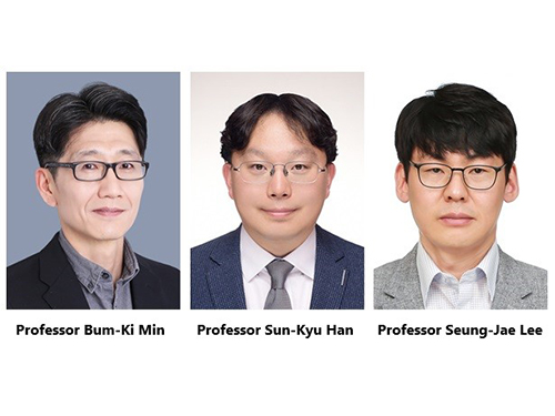
Three KAIST professors swept the 2nd Han Sung Science Awards. Professor Bum-Ki Min from the Departments of Mechanical Engineering and Physics, Professor Sun-Kyu Han from the Department of Chemistry, and Professor Seung-Jae Lee from the Department of Biological Sciences won all three awards presented by the Han Sung Scholarship Foundation, which recognizes promising mid-career scientists in the fields of physics, chemistry, and biological sciences. The awards ceremony will take place on August 16 in Hwaseong.
Professor Min was declared as the winner of the physics field in recognition of his outstanding research activities including searching for new application areas for metamaterials and investigating their unexplored functionalities. The metamaterials with a high index of refraction developed by Professor Min’s research team have caught the attention of scientists worldwide, as they can help develop high-resolution imaging systems and ultra-small, hyper-sensitive optical devices.
The chemistry field winner, Professor Han, is the youngest awardee so far at 36 years of age. He is often described as one of the most promising next-generation Korean scientists in the field of the total synthesis of complex natural products. Given the fact that this field takes very long-term research, he is making unprecedented research achievements. He is focusing on convergent and flexible synthetic approaches that enable access to not only a single target but various natural products with structural and biosynthetic relevance as well as unnatural products with higher biological potency.
Professor Lee was recognized for his contributions to the advancement of biological sciences, especially in aging research. Professor Lee’s team is taking a novel approach by further investigating complex interactions between genetic and environmental factors that affect aging, and identifying genes that mediate the effects. The team has been conducting large-scale gene discovery efforts by employing RNA sequencing analysis, RNAi screening, and chemical mutagenesis screening. They are striving to determine the functional significance of candidate genes obtained from these experiments and mechanistically characterize these genes.
(END)
2019.07.03 View 10580
Three Professors Receive Han Sung Science Awards
Three KAIST professors swept the 2nd Han Sung Science Awards. Professor Bum-Ki Min from the Departments of Mechanical Engineering and Physics, Professor Sun-Kyu Han from the Department of Chemistry, and Professor Seung-Jae Lee from the Department of Biological Sciences won all three awards presented by the Han Sung Scholarship Foundation, which recognizes promising mid-career scientists in the fields of physics, chemistry, and biological sciences. The awards ceremony will take place on August 16 in Hwaseong.
Professor Min was declared as the winner of the physics field in recognition of his outstanding research activities including searching for new application areas for metamaterials and investigating their unexplored functionalities. The metamaterials with a high index of refraction developed by Professor Min’s research team have caught the attention of scientists worldwide, as they can help develop high-resolution imaging systems and ultra-small, hyper-sensitive optical devices.
The chemistry field winner, Professor Han, is the youngest awardee so far at 36 years of age. He is often described as one of the most promising next-generation Korean scientists in the field of the total synthesis of complex natural products. Given the fact that this field takes very long-term research, he is making unprecedented research achievements. He is focusing on convergent and flexible synthetic approaches that enable access to not only a single target but various natural products with structural and biosynthetic relevance as well as unnatural products with higher biological potency.
Professor Lee was recognized for his contributions to the advancement of biological sciences, especially in aging research. Professor Lee’s team is taking a novel approach by further investigating complex interactions between genetic and environmental factors that affect aging, and identifying genes that mediate the effects. The team has been conducting large-scale gene discovery efforts by employing RNA sequencing analysis, RNAi screening, and chemical mutagenesis screening. They are striving to determine the functional significance of candidate genes obtained from these experiments and mechanistically characterize these genes.
(END)
2019.07.03 View 10580 -
 Efficiently Producing Fatty Acids and Biofuels from Glucose
Researchers have presented a new strategy for efficiently producing fatty acids and biofuels that can transform glucose and oleaginous microorganisms into microbial diesel fuel, with one-step direct fermentative production.
The newly developed strain, created by Distinguished Professor Sang Yup Lee and his team, showed the highest efficiency in producing fatty acids and biodiesels ever reported. It will be expected to serve as a new platform to sustainably produce a wide array of fatty acid-based products from glucose and other carbon substrates.
Fossil fuels, which have long been energy resources for our daily lives, are now facing serious challenges: depletion of their reserves and their role in global warming. The production of sustainable bio-based renewable energy has emerged as an essential alternative and many studies to replace fossil fuels are underway. One of the representative examples is biodiesel. Currently, it is mainly being produced through the transesterification of vegetable oils or animal fats.
The research team engineered oleaginous microorganisms, Rhodococcus opacus, to produce fatty acids and their derivatives that can be used as biodiesel from glucose, one of the most abundant and cheap sugars derived from non-edible biomass.
Professor Lee’s team has already engineered Escherichia coli to produce short-chain hydrocarbons, which can be used as gasoline (published in Nature as the cover paper in 2013). However, the production efficiency of the short-chain hydrocarbons using E. coli (0.58 g/L) fell short of the levels required for commercialization.
To overcome these issues, the team employed oil-accumulating Rhodococcus opacus as a host strain in this study. First, the team optimized the cultivation conditions of Rhodococcus opacus to maximize the accumulation of oil (triacylglycerol), which serves as a precursor for the biosynthesis of fatty acids and their derivatives. Then, they systematically analyzed the metabolism of the strain and redesigned it to enable higher levels of fatty acids and two kinds of fatty acid-derived biodiesels (fatty acid ethyl esters and long-chain hydrocarbons) to be produced.
They found that the resulting strains produced 50.2, 21.3, and 5.2 g/L of fatty acids, fatty acid ethyl esters, and long-chain hydrocarbons, respectively. These are all the highest concentrations ever reported by microbial fermentations. It is expected that these strains can contribute to the future industrialization of microbial-based biodiesel production.
“This technology creates fatty acids and biodiesel with high efficiency by utilizing lignocellulose, one of the most abundant resources on the Earth, without depending on fossil fuels and vegetable or animal oils. This will provide new opportunities for oil and petroleum industries, which have long relied on fossil fuels, to turn to sustainable and eco-friendly biotechnologies,” said Professor Lee.
This paper titled “Engineering of an oleaginous bacterium for the production of fatty acids and fuels” was published in Nature Chemical Biology on June 17.
This work was supported by the Technology Development Program to Solve Climate Changes on Systems Metabolic Engineering for Biorefineries from the Ministry of Science and ICT through the National Research Foundation (NRF) of Korea (NRF-2012M1A2A2026556 and NRF-2012M1A2A2026557).
(Figure: Metabolic engineering for the production of free fatty acids (FFAs), fatty acid ethyl esters (FAEEs), and long-chain hydrocarbons (LCHCs) in Rhodococcus opacus PD630. Researchers have presented a new strategy for efficiently producing fatty acids and biofuels that can transform glucose and oleaginous microorganisms into microbial diesel fuel, with one-step direct fermentative production.)
# # #
Source:
Hye Mi Kim, Tong Un Chae, So Young Choi, Won Jun Kim and Sang Yup Lee. Engineering of an oleaginous bacterium for the production of fatty acids and fuels. Nature Chemical Biology ( https://www.nature.com/nchembio/ ) DOI: 10.1038/s41589-019-0295-5
Profile
Dr. Sang Yup Lee
leesy@kaist.ac.kr
Distinguished Professor at the Department of Chemical and Biomolecular Engineering
KAIST
2019.06.19 View 50525
Efficiently Producing Fatty Acids and Biofuels from Glucose
Researchers have presented a new strategy for efficiently producing fatty acids and biofuels that can transform glucose and oleaginous microorganisms into microbial diesel fuel, with one-step direct fermentative production.
The newly developed strain, created by Distinguished Professor Sang Yup Lee and his team, showed the highest efficiency in producing fatty acids and biodiesels ever reported. It will be expected to serve as a new platform to sustainably produce a wide array of fatty acid-based products from glucose and other carbon substrates.
Fossil fuels, which have long been energy resources for our daily lives, are now facing serious challenges: depletion of their reserves and their role in global warming. The production of sustainable bio-based renewable energy has emerged as an essential alternative and many studies to replace fossil fuels are underway. One of the representative examples is biodiesel. Currently, it is mainly being produced through the transesterification of vegetable oils or animal fats.
The research team engineered oleaginous microorganisms, Rhodococcus opacus, to produce fatty acids and their derivatives that can be used as biodiesel from glucose, one of the most abundant and cheap sugars derived from non-edible biomass.
Professor Lee’s team has already engineered Escherichia coli to produce short-chain hydrocarbons, which can be used as gasoline (published in Nature as the cover paper in 2013). However, the production efficiency of the short-chain hydrocarbons using E. coli (0.58 g/L) fell short of the levels required for commercialization.
To overcome these issues, the team employed oil-accumulating Rhodococcus opacus as a host strain in this study. First, the team optimized the cultivation conditions of Rhodococcus opacus to maximize the accumulation of oil (triacylglycerol), which serves as a precursor for the biosynthesis of fatty acids and their derivatives. Then, they systematically analyzed the metabolism of the strain and redesigned it to enable higher levels of fatty acids and two kinds of fatty acid-derived biodiesels (fatty acid ethyl esters and long-chain hydrocarbons) to be produced.
They found that the resulting strains produced 50.2, 21.3, and 5.2 g/L of fatty acids, fatty acid ethyl esters, and long-chain hydrocarbons, respectively. These are all the highest concentrations ever reported by microbial fermentations. It is expected that these strains can contribute to the future industrialization of microbial-based biodiesel production.
“This technology creates fatty acids and biodiesel with high efficiency by utilizing lignocellulose, one of the most abundant resources on the Earth, without depending on fossil fuels and vegetable or animal oils. This will provide new opportunities for oil and petroleum industries, which have long relied on fossil fuels, to turn to sustainable and eco-friendly biotechnologies,” said Professor Lee.
This paper titled “Engineering of an oleaginous bacterium for the production of fatty acids and fuels” was published in Nature Chemical Biology on June 17.
This work was supported by the Technology Development Program to Solve Climate Changes on Systems Metabolic Engineering for Biorefineries from the Ministry of Science and ICT through the National Research Foundation (NRF) of Korea (NRF-2012M1A2A2026556 and NRF-2012M1A2A2026557).
(Figure: Metabolic engineering for the production of free fatty acids (FFAs), fatty acid ethyl esters (FAEEs), and long-chain hydrocarbons (LCHCs) in Rhodococcus opacus PD630. Researchers have presented a new strategy for efficiently producing fatty acids and biofuels that can transform glucose and oleaginous microorganisms into microbial diesel fuel, with one-step direct fermentative production.)
# # #
Source:
Hye Mi Kim, Tong Un Chae, So Young Choi, Won Jun Kim and Sang Yup Lee. Engineering of an oleaginous bacterium for the production of fatty acids and fuels. Nature Chemical Biology ( https://www.nature.com/nchembio/ ) DOI: 10.1038/s41589-019-0295-5
Profile
Dr. Sang Yup Lee
leesy@kaist.ac.kr
Distinguished Professor at the Department of Chemical and Biomolecular Engineering
KAIST
2019.06.19 View 50525 -
 Real-Time Analysis of MOF Adsorption Behavior
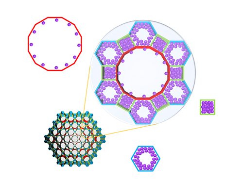
Researchers have developed a technology to analyze the adsorption behavior of molecules in each individual pore of a metal organic framework (MOF). This system has large specific surface areas, allowing for the real-time observation of the adsorption process of an MOF, a new material effective for sorting carbon dioxide, hydrogen, and methane.
Accurate measurements and assessments of gas adsorption isotherms are important for characterizing porous materials and developing their applications. The existing technology is only able to measure the amount of gas molecules adsorbed to the material, without directly observing the adsorption behavior.
The research team led by Professor Jeung Ku Kang from the Graduate School of Energy, Environment, Water and Sustainability (EEWS) prescribed a real time gas adsorption crystallography system by integrating an existing X-ray diffraction (XRD) measurement device that can provide structural information and a gas adsorption measurement device.
Specifically, the system allowed the observation of a mesoporous MOF that has multiple pores rather than a single pore structure. The research team categorized the adsorption behaviors of MOF molecules by pore type, followed by observations and measurements, resulting in the identification of a stepwise adsorption process that was previously not possible to analyze.
Further, the team systematically and quantitatively analyzed how the pore structure and the type of adsorption molecule affect the adsorption behavior to suggest what type of MOF structure is appropriate as a storage material for each type of adsorption behavior.
Professor Kang said, “We quantitatively analyzed each pore molecule in real time to identify the effects of chemical and structural properties of pores on adsorption behavior.” He continued, “By understanding the real-time adsorption behavior of molecules at the level of the pores that form the material, rather than the whole material, we will be able to apply this technology to develop a new high-capacity storage material.”
This research was published in Nature Chemistry online on May 13, 2019 under the title ‘Isotherms of Individual Pores by Gas Adsorption Crystallography’.
(Figure. Schematic illustration of molecules adsorbed on metal organic frameworks with different pores of various structures, where the In-situ X-ray crystallography has been developed to classify each pore structure and analyze the position of the molecule to determine the amount of molecules adsorbed to each pore.)
2019.06.18 View 39681
Real-Time Analysis of MOF Adsorption Behavior
Researchers have developed a technology to analyze the adsorption behavior of molecules in each individual pore of a metal organic framework (MOF). This system has large specific surface areas, allowing for the real-time observation of the adsorption process of an MOF, a new material effective for sorting carbon dioxide, hydrogen, and methane.
Accurate measurements and assessments of gas adsorption isotherms are important for characterizing porous materials and developing their applications. The existing technology is only able to measure the amount of gas molecules adsorbed to the material, without directly observing the adsorption behavior.
The research team led by Professor Jeung Ku Kang from the Graduate School of Energy, Environment, Water and Sustainability (EEWS) prescribed a real time gas adsorption crystallography system by integrating an existing X-ray diffraction (XRD) measurement device that can provide structural information and a gas adsorption measurement device.
Specifically, the system allowed the observation of a mesoporous MOF that has multiple pores rather than a single pore structure. The research team categorized the adsorption behaviors of MOF molecules by pore type, followed by observations and measurements, resulting in the identification of a stepwise adsorption process that was previously not possible to analyze.
Further, the team systematically and quantitatively analyzed how the pore structure and the type of adsorption molecule affect the adsorption behavior to suggest what type of MOF structure is appropriate as a storage material for each type of adsorption behavior.
Professor Kang said, “We quantitatively analyzed each pore molecule in real time to identify the effects of chemical and structural properties of pores on adsorption behavior.” He continued, “By understanding the real-time adsorption behavior of molecules at the level of the pores that form the material, rather than the whole material, we will be able to apply this technology to develop a new high-capacity storage material.”
This research was published in Nature Chemistry online on May 13, 2019 under the title ‘Isotherms of Individual Pores by Gas Adsorption Crystallography’.
(Figure. Schematic illustration of molecules adsorbed on metal organic frameworks with different pores of various structures, where the In-situ X-ray crystallography has been developed to classify each pore structure and analyze the position of the molecule to determine the amount of molecules adsorbed to each pore.)
2019.06.18 View 39681 -
 Novel Via-Hole-Less Multilevel Metal Interconnection Methods
Forming reliable multi-level metal interconnections is a key technology for integrating devices into organic integrated circuits (ICs). The conventional approach, called “via-hole,” locally removes the insulator and utilizes metal interconnects through the holes. Due to the high sensitivity of organic materials to chemical solvents, heat, and photo-radiation used in conventional “via-hole” methods, alternative printing methods or laser drilling methods have been developed. However, finding a reliable and practical metal interconnection for organic ICs is still challenging.
The research team of KAIST Professor Sung Gap Im and Postech Professor Kim Jae-Joon reported a new interconnection method that does not require via-hole formation, “via-hole-less metal interconnection,” in Nature Communications on June 3.
Metal electrodes in different layers can be isolated from each other by patterned dielectric layers, where they then can be interconnected to others in the open area where the dielectric layer is not present. See the images below. Vapor phase deposition and in-situ patterning of dielectric layer using iCVD (initiated chemical vapor deposition), used in the “via-hole-less” method, ensure a damage-free process for organic semiconductor materials and result in outstanding performance of the organic devices as multilevel metal interconnects are reliably formed. The team successfully demonstrated three-dimensional (3D) stacking of five organic transistors and integrated circuits using the proposed via-hole-less interconnect method. See the image below.
Vapor phase deposition and in-situ patterning of dielectric layer using iCVD (initiated chemical vapor deposition), used in the “via-hole-less” method, ensure a damage-free process for organic semiconductor materials and result in outstanding performance of the organic devices as multilevel metal interconnects are reliably formed. The team successfully demonstrated three-dimensional (3D) stacking of five organic transistors and integrated circuits using the proposed via-hole-less interconnect method. See the image below.
Professor Kim explained, “Our proposed via-hole-less interconnect method using a selectively patterned dielectric overcomes the limitations of the previous time-consuming, one-by-one via-hole formation process and provides reliable methods for creating metal interconnects in organic ICs. We expect the via-hole-less scheme to bring advances to organic IC technology.”
2019.06.18 View 44844
Novel Via-Hole-Less Multilevel Metal Interconnection Methods
Forming reliable multi-level metal interconnections is a key technology for integrating devices into organic integrated circuits (ICs). The conventional approach, called “via-hole,” locally removes the insulator and utilizes metal interconnects through the holes. Due to the high sensitivity of organic materials to chemical solvents, heat, and photo-radiation used in conventional “via-hole” methods, alternative printing methods or laser drilling methods have been developed. However, finding a reliable and practical metal interconnection for organic ICs is still challenging.
The research team of KAIST Professor Sung Gap Im and Postech Professor Kim Jae-Joon reported a new interconnection method that does not require via-hole formation, “via-hole-less metal interconnection,” in Nature Communications on June 3.
Metal electrodes in different layers can be isolated from each other by patterned dielectric layers, where they then can be interconnected to others in the open area where the dielectric layer is not present. See the images below. Vapor phase deposition and in-situ patterning of dielectric layer using iCVD (initiated chemical vapor deposition), used in the “via-hole-less” method, ensure a damage-free process for organic semiconductor materials and result in outstanding performance of the organic devices as multilevel metal interconnects are reliably formed. The team successfully demonstrated three-dimensional (3D) stacking of five organic transistors and integrated circuits using the proposed via-hole-less interconnect method. See the image below.
Vapor phase deposition and in-situ patterning of dielectric layer using iCVD (initiated chemical vapor deposition), used in the “via-hole-less” method, ensure a damage-free process for organic semiconductor materials and result in outstanding performance of the organic devices as multilevel metal interconnects are reliably formed. The team successfully demonstrated three-dimensional (3D) stacking of five organic transistors and integrated circuits using the proposed via-hole-less interconnect method. See the image below.
Professor Kim explained, “Our proposed via-hole-less interconnect method using a selectively patterned dielectric overcomes the limitations of the previous time-consuming, one-by-one via-hole formation process and provides reliable methods for creating metal interconnects in organic ICs. We expect the via-hole-less scheme to bring advances to organic IC technology.”
2019.06.18 View 44844 -
 Nanomaterials Mimicking Natural Enzymes with Superior Catalytic Activity and Selectivity for Detecting Acetylcholine
(Professor Jinwoo Lee from the Department of Chemical and Biomolecular Engineering)
A KAIST research team doped nitrogen and boron into graphene to selectively increase peroxidase-like activity and succeeded in synthesizing a peroxidase-mimicking nanozyme with a low cost and superior catalytic activity. These nanomaterials can be applied for early diagnosis of Alzheimer’s disease.
Enzymes are the main catalysts in our body and are widely used in bioassays. In particular, peroxidase, which oxidizes transparent colorimetric substrates to become a colored product in the presence of hydrogen peroxide, is the most common enzyme that is used in colorimetric bioassays.
However, natural enzymes consisting of proteins are unstable against temperature and pH, hard to synthesize, and costly. Nanozymes, on the other hand, do not consist of proteins, meaning the disadvantages of enzymes can be overcome with their robustness and high productivity. In contrast, most nanonzymes do not have selectivity; for example, peroxidase-mimicking nanozymes demonstrate oxidase-like activity that oxidizes colorimetric substrates in the absence of hydrogen peroxide, which keeps them away from precisely detecting the target materials, such as hydrogen peroxide.
Professor Jinwoo Lee from the Department of Chemical and Biomolecular Engineering and his team were able to synthesize a peroxidase-mimicking nanozyme with superior catalytic activity and selectivity toward hydrogen peroxide. Co-doping of nitrogen and boron into graphene, which has negligible peroxidase-like activity, selectively increased the peroxidase-like activity without oxidase-like activity to accurately mimic the nature peroxidase and has become a powerful candidate to replace the peroxidase.
The experimental results were also verified with computational chemistry. The nitrogen and boron co-doped graphene was also applied to the colorimetric detection of acetylcholine, which is an important neurotransmitter and successfully detected the acetylcholine even better than the nature peroxidase.
Professor Lee said, “We began to study nanozymes due to their potential for replacing existing enzymes. Through this study, we have secured core technologies to synthesize nanozymes that have high enzyme activity along with selectivity. We believe that they can be applied to effectively detect acetylcholine for quickly diagnosing Alzheimer’s disease.
This research, led by PhD Min Su Kim, was published in ACS Nano (10.1021/acsnano.8b09519) on March 25, 2019.
Figure 1. Comparison of the catalytic activities of various nanozymes and horseradish peroxidase (HRP) toward TMB and H₂O₂
Figure 2. Schematic illustration of NB-rGO Reactions in Bioassays
2019.04.30 View 38107
Nanomaterials Mimicking Natural Enzymes with Superior Catalytic Activity and Selectivity for Detecting Acetylcholine
(Professor Jinwoo Lee from the Department of Chemical and Biomolecular Engineering)
A KAIST research team doped nitrogen and boron into graphene to selectively increase peroxidase-like activity and succeeded in synthesizing a peroxidase-mimicking nanozyme with a low cost and superior catalytic activity. These nanomaterials can be applied for early diagnosis of Alzheimer’s disease.
Enzymes are the main catalysts in our body and are widely used in bioassays. In particular, peroxidase, which oxidizes transparent colorimetric substrates to become a colored product in the presence of hydrogen peroxide, is the most common enzyme that is used in colorimetric bioassays.
However, natural enzymes consisting of proteins are unstable against temperature and pH, hard to synthesize, and costly. Nanozymes, on the other hand, do not consist of proteins, meaning the disadvantages of enzymes can be overcome with their robustness and high productivity. In contrast, most nanonzymes do not have selectivity; for example, peroxidase-mimicking nanozymes demonstrate oxidase-like activity that oxidizes colorimetric substrates in the absence of hydrogen peroxide, which keeps them away from precisely detecting the target materials, such as hydrogen peroxide.
Professor Jinwoo Lee from the Department of Chemical and Biomolecular Engineering and his team were able to synthesize a peroxidase-mimicking nanozyme with superior catalytic activity and selectivity toward hydrogen peroxide. Co-doping of nitrogen and boron into graphene, which has negligible peroxidase-like activity, selectively increased the peroxidase-like activity without oxidase-like activity to accurately mimic the nature peroxidase and has become a powerful candidate to replace the peroxidase.
The experimental results were also verified with computational chemistry. The nitrogen and boron co-doped graphene was also applied to the colorimetric detection of acetylcholine, which is an important neurotransmitter and successfully detected the acetylcholine even better than the nature peroxidase.
Professor Lee said, “We began to study nanozymes due to their potential for replacing existing enzymes. Through this study, we have secured core technologies to synthesize nanozymes that have high enzyme activity along with selectivity. We believe that they can be applied to effectively detect acetylcholine for quickly diagnosing Alzheimer’s disease.
This research, led by PhD Min Su Kim, was published in ACS Nano (10.1021/acsnano.8b09519) on March 25, 2019.
Figure 1. Comparison of the catalytic activities of various nanozymes and horseradish peroxidase (HRP) toward TMB and H₂O₂
Figure 2. Schematic illustration of NB-rGO Reactions in Bioassays
2019.04.30 View 38107 -
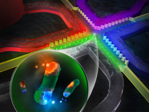 On-chip Drug Screening for Identifying Antibiotic Interactions in Eight Hours
(from left: Seunggyu Kimand Professor Jessie Sungyun Jeon)
A KAIST research team developed a microfluidic-based drug screening chip that identifies synergistic interactions between two antibiotics in eight hours. This chip can be a cell-based drug screening platform for exploring critical pharmacological patterns of antibiotic interactions, along with potential applications in screening other cell-type agents and guidance for clinical therapies.
Antibiotic susceptibility testing, which determines types and doses of antibiotics that can effectively inhibit bacterial growth, has become more critical in recent years with the emergence of antibiotic-resistant pathogenic bacteria strains.
To overcome the antibiotic-resistant bacteria, combinatory therapy using two or more kinds of antibiotics has been gaining considerable attention. However, the major problem is that this therapy is not always effective; occasionally, unfavorable antibiotic pairs may worsen results, leading to suppressed antimicrobial effects. Therefore, combinatory testing is a crucial preliminary process to find suitable antibiotic pairs and their concentration range against unknown pathogens, but the conventional testing methods are inconvenient for concentration dilution and sample preparation, and they take more than 24 hours to produce the results.
To reduce time and enhance the efficiency of combinatory testing, Professor Jessie Sungyun Jeon from the Department of Mechanical Engineering, in collaboration with Professor Hyun Jung Chung from the Department of Biological Sciences, developed a high-throughput drug screening chip that generates 121 pairwise concentrations between two antibiotics.
The team utilized a microfluidic chip with a sample volume of a few tens of microliters. This chip enabled 121 pairwise concentrations of two antibiotics to be automatically formed in only 35 minutes.
They loaded a mixture of bacterial samples and agarose into the microchannel and injected reagents with or without antibiotics into the surrounding microchannel. The diffusion of antibiotic molecules from the channel with antibiotics to the one without antibiotics resulted in the formation of two orthogonal concentration gradients of the two antibiotics on the bacteria-trapping agarose gel.
The team observed the inhibition of bacterial growth by the antibiotic orthogonal gradients over six hours with a microscope, and confirmed different patterns of antibiotic pairs, classifying the interaction types into either synergy or antagonism.
Professor Jeon said, “The feasibility of microfluidic-based drug screening chips is promising, and we expect our microfluidic chip to be commercialized and utilized in near future.”
This study, led by Seunggyu Kim, was published in Lab on a Chip (10.1039/c8lc01406j) on March 21, 2019.
Figure 1. Back cover image for the “Lab on a Chip”.
Figure 2. Examples of testing results using the microfluidic chips developed in this research.
2019.04.18 View 31583
On-chip Drug Screening for Identifying Antibiotic Interactions in Eight Hours
(from left: Seunggyu Kimand Professor Jessie Sungyun Jeon)
A KAIST research team developed a microfluidic-based drug screening chip that identifies synergistic interactions between two antibiotics in eight hours. This chip can be a cell-based drug screening platform for exploring critical pharmacological patterns of antibiotic interactions, along with potential applications in screening other cell-type agents and guidance for clinical therapies.
Antibiotic susceptibility testing, which determines types and doses of antibiotics that can effectively inhibit bacterial growth, has become more critical in recent years with the emergence of antibiotic-resistant pathogenic bacteria strains.
To overcome the antibiotic-resistant bacteria, combinatory therapy using two or more kinds of antibiotics has been gaining considerable attention. However, the major problem is that this therapy is not always effective; occasionally, unfavorable antibiotic pairs may worsen results, leading to suppressed antimicrobial effects. Therefore, combinatory testing is a crucial preliminary process to find suitable antibiotic pairs and their concentration range against unknown pathogens, but the conventional testing methods are inconvenient for concentration dilution and sample preparation, and they take more than 24 hours to produce the results.
To reduce time and enhance the efficiency of combinatory testing, Professor Jessie Sungyun Jeon from the Department of Mechanical Engineering, in collaboration with Professor Hyun Jung Chung from the Department of Biological Sciences, developed a high-throughput drug screening chip that generates 121 pairwise concentrations between two antibiotics.
The team utilized a microfluidic chip with a sample volume of a few tens of microliters. This chip enabled 121 pairwise concentrations of two antibiotics to be automatically formed in only 35 minutes.
They loaded a mixture of bacterial samples and agarose into the microchannel and injected reagents with or without antibiotics into the surrounding microchannel. The diffusion of antibiotic molecules from the channel with antibiotics to the one without antibiotics resulted in the formation of two orthogonal concentration gradients of the two antibiotics on the bacteria-trapping agarose gel.
The team observed the inhibition of bacterial growth by the antibiotic orthogonal gradients over six hours with a microscope, and confirmed different patterns of antibiotic pairs, classifying the interaction types into either synergy or antagonism.
Professor Jeon said, “The feasibility of microfluidic-based drug screening chips is promising, and we expect our microfluidic chip to be commercialized and utilized in near future.”
This study, led by Seunggyu Kim, was published in Lab on a Chip (10.1039/c8lc01406j) on March 21, 2019.
Figure 1. Back cover image for the “Lab on a Chip”.
Figure 2. Examples of testing results using the microfluidic chips developed in this research.
2019.04.18 View 31583 -
 True-meaning Wearable Displays: Self-powered, Washable and Wearable
(Video: The washing process of wearing display module) When we think about clothes, they are usually formed with textiles and have to be both wearable and washable for daily use; however, smart clothing has had a problem with its power sources and moisture permeability, which causes the devices to malfunction. This problem has now been overcome by a KAIST research team, who developed a textile-based wearable display module technology that is washable and does not require an external power source.
To ease out the problem of external power sources and enhance the practicability of wearable displays, Professor Kyung Cheol Choi from the School of Electrical Engineering and his team fabricated their wearing display modules on real textiles that integrated polymer solar cells (PSCs) with organic light emitting diodes (OLEDs).
PSCs have been one of the most promising candidates for a next-generation power source, especially for wearable and optoelectronic applications because they can provide stable power without an external power source, while OLEDs can be driven with milliwatts. However, the problem was that they are both very vulnerable to external moisture and oxygen. The encapsulation barrier is essential for their reliability. The conventional encapsulation barrier is sufficient for normal environments; however, it loses its characteristics in aqueous environments, such as water. It limits the commercialization of wearing displays that must operate even on rainy days or after washing.
To tackle this issue, the team employed a washable encapsulation barrier that can protect the device without losing its characteristics after washing through atomic layer deposition (ALD) and spin coating. With this encapsulation technology, the team confirmed that textile-based wearing display modules including PSCs, OLEDs, and the proposed encapsulation barrier exhibited little change in characteristics even after 20 washings with 10-minute cycles. Moreover, the encapsulated device operated stably with a low curvature radius of 3mm and boasted high reliability.
Finally, it exhibited no deterioration in properties over 30 days even after being subjected to both bending stress and washing. Since it uses a less stressful textile, compared to conventional wearable electronic devices that use traditional plastic substrates, this technology can accelerate the commercialization of wearing electronic devices. Importantly, this wearable electronic device in daily life can save energy through a self-powered system.
Professor Choi said, “I could say that this research realized a truly washable wearable electronic module in the sense that it uses daily wearable textiles instead of the plastic used in conventional wearable electronic devices. Saving energy with PSCs, it can be self-powered, using nature-friendly solar energy, and washed. I believe that it has paved the way for a ‘true-meaning wearable display’ that can be formed on textile, beyond the attachable form of wearable technology.”
This research, in collaboration with Professor Seok Ho Cho from Chonnam National University and led by Eun Gyo Jeong, was published in Energy and Environmental Science (10.1039/c8ee03271h) on January 18, 2019.
Figure 1. Schematic and photo of a washable wearing display module
Figure 2. Cover page of Energy and Environmental Science
2019.03.21 View 31857
True-meaning Wearable Displays: Self-powered, Washable and Wearable
(Video: The washing process of wearing display module) When we think about clothes, they are usually formed with textiles and have to be both wearable and washable for daily use; however, smart clothing has had a problem with its power sources and moisture permeability, which causes the devices to malfunction. This problem has now been overcome by a KAIST research team, who developed a textile-based wearable display module technology that is washable and does not require an external power source.
To ease out the problem of external power sources and enhance the practicability of wearable displays, Professor Kyung Cheol Choi from the School of Electrical Engineering and his team fabricated their wearing display modules on real textiles that integrated polymer solar cells (PSCs) with organic light emitting diodes (OLEDs).
PSCs have been one of the most promising candidates for a next-generation power source, especially for wearable and optoelectronic applications because they can provide stable power without an external power source, while OLEDs can be driven with milliwatts. However, the problem was that they are both very vulnerable to external moisture and oxygen. The encapsulation barrier is essential for their reliability. The conventional encapsulation barrier is sufficient for normal environments; however, it loses its characteristics in aqueous environments, such as water. It limits the commercialization of wearing displays that must operate even on rainy days or after washing.
To tackle this issue, the team employed a washable encapsulation barrier that can protect the device without losing its characteristics after washing through atomic layer deposition (ALD) and spin coating. With this encapsulation technology, the team confirmed that textile-based wearing display modules including PSCs, OLEDs, and the proposed encapsulation barrier exhibited little change in characteristics even after 20 washings with 10-minute cycles. Moreover, the encapsulated device operated stably with a low curvature radius of 3mm and boasted high reliability.
Finally, it exhibited no deterioration in properties over 30 days even after being subjected to both bending stress and washing. Since it uses a less stressful textile, compared to conventional wearable electronic devices that use traditional plastic substrates, this technology can accelerate the commercialization of wearing electronic devices. Importantly, this wearable electronic device in daily life can save energy through a self-powered system.
Professor Choi said, “I could say that this research realized a truly washable wearable electronic module in the sense that it uses daily wearable textiles instead of the plastic used in conventional wearable electronic devices. Saving energy with PSCs, it can be self-powered, using nature-friendly solar energy, and washed. I believe that it has paved the way for a ‘true-meaning wearable display’ that can be formed on textile, beyond the attachable form of wearable technology.”
This research, in collaboration with Professor Seok Ho Cho from Chonnam National University and led by Eun Gyo Jeong, was published in Energy and Environmental Science (10.1039/c8ee03271h) on January 18, 2019.
Figure 1. Schematic and photo of a washable wearing display module
Figure 2. Cover page of Energy and Environmental Science
2019.03.21 View 31857 -
 Wafer-Scale Multilayer Fabrication of Silk Fibroin-Based Microelectronics
A KAIST research team developed a novel fabrication method for the multilayer processing of silk-based microelectronics. This technology for creating a biodegradable silk fibroin film allows microfabrication with polymer or metal structures manufactured from photolithography. It can be a key technology in the implementation of silk fibroin-based biodegradable electronic devices or localized drug delivery through silk fibroin patterns.
Silk fibroins are biocompatible, biodegradable, transparent, and flexible, which makes them excellent candidates for implantable biomedical devices, and they have also been used as biodegradable films and functional microstructures in biomedical applications. However, conventional microfabrication processes require strong etching solutions and solvents to modify the structure of silk fibroins.
To prevent the silk fibroin from being damaged during the process, Professor Hyunjoo J. Lee from the School of Electrical Engineering and her team came up with a novel process, named aluminum hard mask on silk fibroin (AMoS), which is capable of micropatterning multiple layers composed of both fibroin and inorganic materials, such as metal and dielectrics with high-precision microscale alignment. The AMoS process can make silk fibroin patterns on devices, or make patterns on silk fibroin thin films with other materials by using photolithography, which is a core technology in the current microfabrication process.
The team successfully cultured primary neurons on the processed silk fibroin micro-patterns, and confirmed that silk fibroin has excellent biocompatibility before and after the fabrication process and that it also can be applied to implanted biological devices.
Through this technology, the team realized the multilayer micropatterning of fibroin films on a silk fibroin substrate and fabricated a biodegradable microelectric circuit consisting of resistors and silk fibroin dielectric capacitors in a silicon wafer with large areas.
They also used this technology to position the micro-pattern of the silk fibroin thin film closer to the flexible polymer-based brain electrode, and confirmed the dye molecules mounted on the silk fibroin were transferred successfully from the micropatterns.
Professor Lee said, “This technology facilitates wafer-scale, large-area processing of sensitive materials. We expect it to be applied to a wide range of biomedical devices in the future. Using the silk fibroin with micro-patterned brain electrodes can open up many new possibilities in research on brain circuits by mounting drugs that restrict or promote brain cell activities.”
This research, in collaboration with Dr. Nakwon Choi from KIST and led by PhD candidate Geon Kook, was published in ACS AMI (10.1021/acsami.8b13170) on January 16, 2019.
Figure 1. The cover page of ACS AMI
Figure 2. Fibroin microstructures and metal patterns on a fibroin produced by using the AMoS mask.
Figure 3. Biocompatibility assessment of the AMoS Process. Top: Schematics image of a) fibroin-coated silicon b) fibroin-pattered silicon and c) gold-patterned fibroin. Bottom: Representative confocal microscopy images of live (green) and dead (red) primary cortical neurons cultured on the substrates.
2019.03.15 View 23088
Wafer-Scale Multilayer Fabrication of Silk Fibroin-Based Microelectronics
A KAIST research team developed a novel fabrication method for the multilayer processing of silk-based microelectronics. This technology for creating a biodegradable silk fibroin film allows microfabrication with polymer or metal structures manufactured from photolithography. It can be a key technology in the implementation of silk fibroin-based biodegradable electronic devices or localized drug delivery through silk fibroin patterns.
Silk fibroins are biocompatible, biodegradable, transparent, and flexible, which makes them excellent candidates for implantable biomedical devices, and they have also been used as biodegradable films and functional microstructures in biomedical applications. However, conventional microfabrication processes require strong etching solutions and solvents to modify the structure of silk fibroins.
To prevent the silk fibroin from being damaged during the process, Professor Hyunjoo J. Lee from the School of Electrical Engineering and her team came up with a novel process, named aluminum hard mask on silk fibroin (AMoS), which is capable of micropatterning multiple layers composed of both fibroin and inorganic materials, such as metal and dielectrics with high-precision microscale alignment. The AMoS process can make silk fibroin patterns on devices, or make patterns on silk fibroin thin films with other materials by using photolithography, which is a core technology in the current microfabrication process.
The team successfully cultured primary neurons on the processed silk fibroin micro-patterns, and confirmed that silk fibroin has excellent biocompatibility before and after the fabrication process and that it also can be applied to implanted biological devices.
Through this technology, the team realized the multilayer micropatterning of fibroin films on a silk fibroin substrate and fabricated a biodegradable microelectric circuit consisting of resistors and silk fibroin dielectric capacitors in a silicon wafer with large areas.
They also used this technology to position the micro-pattern of the silk fibroin thin film closer to the flexible polymer-based brain electrode, and confirmed the dye molecules mounted on the silk fibroin were transferred successfully from the micropatterns.
Professor Lee said, “This technology facilitates wafer-scale, large-area processing of sensitive materials. We expect it to be applied to a wide range of biomedical devices in the future. Using the silk fibroin with micro-patterned brain electrodes can open up many new possibilities in research on brain circuits by mounting drugs that restrict or promote brain cell activities.”
This research, in collaboration with Dr. Nakwon Choi from KIST and led by PhD candidate Geon Kook, was published in ACS AMI (10.1021/acsami.8b13170) on January 16, 2019.
Figure 1. The cover page of ACS AMI
Figure 2. Fibroin microstructures and metal patterns on a fibroin produced by using the AMoS mask.
Figure 3. Biocompatibility assessment of the AMoS Process. Top: Schematics image of a) fibroin-coated silicon b) fibroin-pattered silicon and c) gold-patterned fibroin. Bottom: Representative confocal microscopy images of live (green) and dead (red) primary cortical neurons cultured on the substrates.
2019.03.15 View 23088 -
 KAIST Develops Analog Memristive Synapses for Neuromorphic Chips
(Professor Sung-Yool Choi from the School of Electrical Engineering)
A KAIST research team developed a technology that makes a transition of the operation mode of flexible memristors to synaptic analog switching by reducing the size of the formed filament. Through this technology, memristors can extend their role to memristive synapses for neuromorphic chips, which will lead to developing soft neuromorphic intelligent systems.
Brain-inspired neuromorphic chips have been gaining a great deal of attention for reducing the power consumption and integrating data processing, compared to conventional semiconductor chips. Similarly, memristors are known to be the most suitable candidate for making a crossbar array which is the most efficient architecture for realizing hardware-based artificial neural network (ANN) inside a neuromorphic chip.
A hardware-based ANN consists of a neuron circuit and synapse elements, the connecting pieces. In the neuromorphic system, the synaptic weight, which represents the connection strength between neurons, should be stored and updated as the type of analog data at each synapse.
However, most memristors have digital characteristics suitable for nonvolatile memory. These characteristics put a limitation on the analog operation of the memristors, which makes it difficult to apply them to synaptic devices.
Professor Sung-Yool Choi from the School of Electrical Engineering and his team fabricated a flexible polymer memristor on a plastic substrate, and found that changing the size of the conductive metal filaments formed inside the device on the scale of metal atoms can make a transition of the memristor behavior from digital to analog.
Using this phenomenon, the team developed flexible memristor-based electronic synapses, which can continuously and linearly update synaptic weight, and operate under mechanical deformations such as bending.
The team confirmed that the ANN based on these memristor synapses can effectively classify person’s facial images even when they were damaged. This research demonstrated the possibility of a neuromorphic chip that can efficiently recognize faces, numbers, and objects.
Professor Choi said, “We found the principles underlying the transition from digital to analog operation of the memristors. I believe that this research paves the way for applying various memristors to either digital memory or electronic synapses, and will accelerate the development of a high-performing neuromorphic chip.”
In a joint research project with Professor Sung Gap Im (KAIST) and Professor V. P. Dravid (Northwestern University), this study was led by Dr. Byung Chul Jang (Samsung Electronics), Dr. Sungkyu Kim (Northwestern University) and Dr. Sang Yoon Yang (KAIST), and was published online in Nano Letters (10.1021/acs.nanolett.8b04023) on January 4, 2019.
Figure 1. a) Schematic illustration of a flexible pV3D3 memristor-based electronic synapse array. b) Cross-sectional TEM image of the flexible pV3D3 memristor
2019.02.28 View 10222
KAIST Develops Analog Memristive Synapses for Neuromorphic Chips
(Professor Sung-Yool Choi from the School of Electrical Engineering)
A KAIST research team developed a technology that makes a transition of the operation mode of flexible memristors to synaptic analog switching by reducing the size of the formed filament. Through this technology, memristors can extend their role to memristive synapses for neuromorphic chips, which will lead to developing soft neuromorphic intelligent systems.
Brain-inspired neuromorphic chips have been gaining a great deal of attention for reducing the power consumption and integrating data processing, compared to conventional semiconductor chips. Similarly, memristors are known to be the most suitable candidate for making a crossbar array which is the most efficient architecture for realizing hardware-based artificial neural network (ANN) inside a neuromorphic chip.
A hardware-based ANN consists of a neuron circuit and synapse elements, the connecting pieces. In the neuromorphic system, the synaptic weight, which represents the connection strength between neurons, should be stored and updated as the type of analog data at each synapse.
However, most memristors have digital characteristics suitable for nonvolatile memory. These characteristics put a limitation on the analog operation of the memristors, which makes it difficult to apply them to synaptic devices.
Professor Sung-Yool Choi from the School of Electrical Engineering and his team fabricated a flexible polymer memristor on a plastic substrate, and found that changing the size of the conductive metal filaments formed inside the device on the scale of metal atoms can make a transition of the memristor behavior from digital to analog.
Using this phenomenon, the team developed flexible memristor-based electronic synapses, which can continuously and linearly update synaptic weight, and operate under mechanical deformations such as bending.
The team confirmed that the ANN based on these memristor synapses can effectively classify person’s facial images even when they were damaged. This research demonstrated the possibility of a neuromorphic chip that can efficiently recognize faces, numbers, and objects.
Professor Choi said, “We found the principles underlying the transition from digital to analog operation of the memristors. I believe that this research paves the way for applying various memristors to either digital memory or electronic synapses, and will accelerate the development of a high-performing neuromorphic chip.”
In a joint research project with Professor Sung Gap Im (KAIST) and Professor V. P. Dravid (Northwestern University), this study was led by Dr. Byung Chul Jang (Samsung Electronics), Dr. Sungkyu Kim (Northwestern University) and Dr. Sang Yoon Yang (KAIST), and was published online in Nano Letters (10.1021/acs.nanolett.8b04023) on January 4, 2019.
Figure 1. a) Schematic illustration of a flexible pV3D3 memristor-based electronic synapse array. b) Cross-sectional TEM image of the flexible pV3D3 memristor
2019.02.28 View 10222 -
 Stretchable Multi-functional Fiber for Energy Harvesting and Strain Sensing
(from left: Professor Steve Park, Jeongjae Ryu and Professor Seungbum Hong)
Fiber-based electronics are expected to play a vital role in next-generation wearable electronics. Woven into textiles, they can provide higher durability, comfort, and integrated multi-functionality. A KAIST team has developed a stretchable multi-functional fiber (SMF) that can harvest energy and detect strain, which can be applied to future wearable electronics.
With wearable electronics, health and physical conditions can be assessed by analyzing biological signals from the human body, such as pulse and muscle movements. Fibers are highly suitable for future wearable electronics because they can be easily integrated into textiles, which are designed to be conformable to curvilinear surfaces and comfortable to wear. Moreover, their weave structures offer support that makes them resistant to fatigue. Many research groups have developed fiber-based strain sensors to sense external biological signals. However, their sensitivities were relatively low.
The applicability of wearable devices is currently limited by their power source, as the size, weight, and lifetime of the battery lessens their versatility. Harvesting mechanical energy from the human body is a promising solution to overcome such limitations by utilizing various types of motions like bending, stretching, and pressing. However, previously reported, fiber-based energy harvesters were not stretchable and could not fully harvest the available mechanical energy.
Professor Seungbum Hong and Professor Steve Park from the Department of Materials Science and Engineering and their team fabricated a stretchable fiber by using a ferroelectric layer composed of P(VDF-TrFE)/PDMS sandwiched between stretchable electrodes composed of a composite of multi-walled carbon nanotubes (MWCNT) and poly 3,4-ethylenedioxythiophene polystyrenesulfonate (PEDOT:PSS).
Cracks formed in MWCNT/PEDOT:PSS layer help the fiber show high sensitivity compared to the previously reported fiber strain sensors. Furthermore, the new fiber can harvest mechanical energy under various mechanical stimuli such as stretching, tapping, and injecting water into the fiber using the piezoelectric effect of the P(VDF-TrFE)/PDMS layer.
Professor Hong said, “This new fiber has various functionalities and makes the device simple and compact. It is a core technology for developing wearable devices with energy harvesting and strain sensing capabilities.”
This article, led by PhD candidate Jeongjae Ryu, was published in the January 2019 issue of Nano Energy.
Figure 1.Schematic illustration of an SMF fiber and its piezoelectric voltage output and response to strain.
Figure 2. Photographs of a stretchable multi-functional fiber being stretched by 100%, bent, and twisted.
2019.01.31 View 9365
Stretchable Multi-functional Fiber for Energy Harvesting and Strain Sensing
(from left: Professor Steve Park, Jeongjae Ryu and Professor Seungbum Hong)
Fiber-based electronics are expected to play a vital role in next-generation wearable electronics. Woven into textiles, they can provide higher durability, comfort, and integrated multi-functionality. A KAIST team has developed a stretchable multi-functional fiber (SMF) that can harvest energy and detect strain, which can be applied to future wearable electronics.
With wearable electronics, health and physical conditions can be assessed by analyzing biological signals from the human body, such as pulse and muscle movements. Fibers are highly suitable for future wearable electronics because they can be easily integrated into textiles, which are designed to be conformable to curvilinear surfaces and comfortable to wear. Moreover, their weave structures offer support that makes them resistant to fatigue. Many research groups have developed fiber-based strain sensors to sense external biological signals. However, their sensitivities were relatively low.
The applicability of wearable devices is currently limited by their power source, as the size, weight, and lifetime of the battery lessens their versatility. Harvesting mechanical energy from the human body is a promising solution to overcome such limitations by utilizing various types of motions like bending, stretching, and pressing. However, previously reported, fiber-based energy harvesters were not stretchable and could not fully harvest the available mechanical energy.
Professor Seungbum Hong and Professor Steve Park from the Department of Materials Science and Engineering and their team fabricated a stretchable fiber by using a ferroelectric layer composed of P(VDF-TrFE)/PDMS sandwiched between stretchable electrodes composed of a composite of multi-walled carbon nanotubes (MWCNT) and poly 3,4-ethylenedioxythiophene polystyrenesulfonate (PEDOT:PSS).
Cracks formed in MWCNT/PEDOT:PSS layer help the fiber show high sensitivity compared to the previously reported fiber strain sensors. Furthermore, the new fiber can harvest mechanical energy under various mechanical stimuli such as stretching, tapping, and injecting water into the fiber using the piezoelectric effect of the P(VDF-TrFE)/PDMS layer.
Professor Hong said, “This new fiber has various functionalities and makes the device simple and compact. It is a core technology for developing wearable devices with energy harvesting and strain sensing capabilities.”
This article, led by PhD candidate Jeongjae Ryu, was published in the January 2019 issue of Nano Energy.
Figure 1.Schematic illustration of an SMF fiber and its piezoelectric voltage output and response to strain.
Figure 2. Photographs of a stretchable multi-functional fiber being stretched by 100%, bent, and twisted.
2019.01.31 View 9365