Jeong+Young+Park
-
 KAIST Designs a New Atomic Catalyst for Air Pollution Reduction
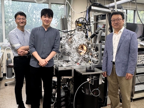
<(From Left)Professor Jong Hun Kim from Inha University, Dr. Gyuho Han and Professor Jeong Young Park from KAIST>
Platinum diselenide (PtSe2) is a two-dimensional multilayer material in which each layer is composed of platinum (Pt) and selenium (Se). It is known that its excellent crystallinity and precise control of interlayer interactions allow modulation of various physical and chemical properties. Due to these characteristics, it has been actively researched in multiple fields, including semiconductors, photodetectors, and electrochemical devices. Now, a research team has proposed a new design concept in which atomically dispersed platinum on the surface of platinum diselenide can function as a catalyst for gas reactions. Through this, they have proven its potential as a next-generation gas-phase catalyst technology for high-efficiency carbon dioxide conversion and carbon monoxide reduction.
KAIST (President Kwang Hyung Lee) announced on July 22 that a joint research team led by Endowed Chair Professor Jeong Young Park from the Department of Chemistry, along with Professor Hyun You Kim's team from Chungnam National University and Professor Yeonwoong (Eric) Jung's team from the University of Central Florida (UCF), has achieved excellent carbon monoxide oxidation performance by utilizing platinum atoms exposed on the surface of platinum diselenide, a type of two-dimensional transition metal dichalcogenide (TMD).
To maximize catalytic performance, the research team designed the catalyst by dispersing platinum atoms uniformly across the surface, departing from the conventional use of bulk platinum. This strategy allows more efficient catalytic reactions using a smaller amount of platinum. It also enhances electronic interactions between platinum and selenium by tuning the surface electronic structure. As a result, the platinum diselenide film with a thickness of a few nanometers showed superior carbon monoxide oxidation performance across the entire temperature range compared to a conventional platinum thin film under identical conditions.
In particular, carbon monoxide and oxygen were evenly adsorbed on the surface in similar proportions, increasing the likelihood that they would encounter each other and react, which significantly enhanced the catalytic activity. This improvement is primarily attributed to the increased exposure of surface platinum atoms resulting from selenium vacancies (Se-vacancies), which provide adsorption sites for gas molecules.
The research team confirmed in real-time that these platinum atoms served as active adsorption sites during the actual reaction process, using ambient-pressure X-ray photoelectron spectroscopy (AP-XPS) conducted at the Pohang Accelerator Laboratory. This high-precision analysis was enabled by advanced instrumentation capable of observing surfaces at the nanometer scale under ambient pressure conditions. At the same time, computer simulations based on density functional theory (DFT) demonstrated that platinum diselenide exhibits distinct electronic behavior compared to conventional platinum.
*Density Functional Theory (DFT): A quantum mechanical method for calculating the total energy of a system based on electron density.
Professor Jeong Young Park stated, “This research presents a new design strategy that utilizes platinum diselenide, a two-dimensional layered material distinct from conventional platinum catalysts, to enable catalytic functions optimized for gas-phase reactions.” He added, “The electronic interaction between platinum and selenium created favorable conditions for the balanced adsorption of carbon monoxide and oxygen. By designing the catalyst to exhibit higher reactivity across the entire temperature range than conventional platinum, we improved its practical applicability. This enabled a high-efficiency catalytic reaction mechanism through atomic-level design, a two-dimensional material platform, and precise adsorption control.”
This research was co-authored by Dr. Gyuho Han from the Department of Chemistry at KAIST, Dr. Hyuk Choi from the Department of Materials Science and Engineering at Chungnam National University, and Professor Jong Hun Kim from Inha University. The study was published on July 3 in the world-renowned journal Nature Communications.
Paper Title: Enhanced catalytic activity on atomically dispersed PtSe2 two-dimensional layers
DOI: 10.1038/s41467-025-61320-0
This research was supported by the Mid-Career Researcher Program of the Ministry of Science and ICT, the Core Research Institute Program of the Ministry of Education, the National Strategic Technology Materials Development Project, the U.S. National Science Foundation (NSF) CAREER Program, research funding from Inha University, and the Postdoctoral Researcher Program (P3) at UCF. Accelerator-based analysis was conducted in cooperation with the Pohang Accelerator Laboratory and the Korea Basic Science Institute (KBSI).
2025.07.22 View 459
KAIST Designs a New Atomic Catalyst for Air Pollution Reduction
<(From Left)Professor Jong Hun Kim from Inha University, Dr. Gyuho Han and Professor Jeong Young Park from KAIST>
Platinum diselenide (PtSe2) is a two-dimensional multilayer material in which each layer is composed of platinum (Pt) and selenium (Se). It is known that its excellent crystallinity and precise control of interlayer interactions allow modulation of various physical and chemical properties. Due to these characteristics, it has been actively researched in multiple fields, including semiconductors, photodetectors, and electrochemical devices. Now, a research team has proposed a new design concept in which atomically dispersed platinum on the surface of platinum diselenide can function as a catalyst for gas reactions. Through this, they have proven its potential as a next-generation gas-phase catalyst technology for high-efficiency carbon dioxide conversion and carbon monoxide reduction.
KAIST (President Kwang Hyung Lee) announced on July 22 that a joint research team led by Endowed Chair Professor Jeong Young Park from the Department of Chemistry, along with Professor Hyun You Kim's team from Chungnam National University and Professor Yeonwoong (Eric) Jung's team from the University of Central Florida (UCF), has achieved excellent carbon monoxide oxidation performance by utilizing platinum atoms exposed on the surface of platinum diselenide, a type of two-dimensional transition metal dichalcogenide (TMD).
To maximize catalytic performance, the research team designed the catalyst by dispersing platinum atoms uniformly across the surface, departing from the conventional use of bulk platinum. This strategy allows more efficient catalytic reactions using a smaller amount of platinum. It also enhances electronic interactions between platinum and selenium by tuning the surface electronic structure. As a result, the platinum diselenide film with a thickness of a few nanometers showed superior carbon monoxide oxidation performance across the entire temperature range compared to a conventional platinum thin film under identical conditions.
In particular, carbon monoxide and oxygen were evenly adsorbed on the surface in similar proportions, increasing the likelihood that they would encounter each other and react, which significantly enhanced the catalytic activity. This improvement is primarily attributed to the increased exposure of surface platinum atoms resulting from selenium vacancies (Se-vacancies), which provide adsorption sites for gas molecules.
The research team confirmed in real-time that these platinum atoms served as active adsorption sites during the actual reaction process, using ambient-pressure X-ray photoelectron spectroscopy (AP-XPS) conducted at the Pohang Accelerator Laboratory. This high-precision analysis was enabled by advanced instrumentation capable of observing surfaces at the nanometer scale under ambient pressure conditions. At the same time, computer simulations based on density functional theory (DFT) demonstrated that platinum diselenide exhibits distinct electronic behavior compared to conventional platinum.
*Density Functional Theory (DFT): A quantum mechanical method for calculating the total energy of a system based on electron density.
Professor Jeong Young Park stated, “This research presents a new design strategy that utilizes platinum diselenide, a two-dimensional layered material distinct from conventional platinum catalysts, to enable catalytic functions optimized for gas-phase reactions.” He added, “The electronic interaction between platinum and selenium created favorable conditions for the balanced adsorption of carbon monoxide and oxygen. By designing the catalyst to exhibit higher reactivity across the entire temperature range than conventional platinum, we improved its practical applicability. This enabled a high-efficiency catalytic reaction mechanism through atomic-level design, a two-dimensional material platform, and precise adsorption control.”
This research was co-authored by Dr. Gyuho Han from the Department of Chemistry at KAIST, Dr. Hyuk Choi from the Department of Materials Science and Engineering at Chungnam National University, and Professor Jong Hun Kim from Inha University. The study was published on July 3 in the world-renowned journal Nature Communications.
Paper Title: Enhanced catalytic activity on atomically dispersed PtSe2 two-dimensional layers
DOI: 10.1038/s41467-025-61320-0
This research was supported by the Mid-Career Researcher Program of the Ministry of Science and ICT, the Core Research Institute Program of the Ministry of Education, the National Strategic Technology Materials Development Project, the U.S. National Science Foundation (NSF) CAREER Program, research funding from Inha University, and the Postdoctoral Researcher Program (P3) at UCF. Accelerator-based analysis was conducted in cooperation with the Pohang Accelerator Laboratory and the Korea Basic Science Institute (KBSI).
2025.07.22 View 459 -
 KAIST Captures Hot Holes: A Breakthrough in Light-to-Electricity Energy Conversion
When light interacts with metallic nanostructures, it instantaneously generates plasmonic hot carriers, which serve as key intermediates for converting optical energy into high-value energy sources such as electricity and chemical energy. Among these, hot holes play a crucial role in enhancing photoelectrochemical reactions. However, they thermally dissipate within picoseconds (trillionths of a second), making practical applications challenging. Now, a Korean research team has successfully developed a method for sustaining hot holes longer and amplifying their flow, accelerating the commercialization of next-generation, high-efficiency, light-to-energy conversion technologies.
KAIST (represented by President Kwang Hyung Lee) announced on the 12th of March that a research team led by Distinguished Professor Jeong Young Park from the Department of Chemistry, in collaboration with Professor Moonsang Lee from the Department of Materials Science and Engineering at Inha University, has successfully amplified the flow of hot holes and mapped local current distribution in real time, thereby elucidating the mechanism of photocurrent enhancement.
The team designed a nanodiode structure by placing a metallic nanomesh on a specialized semiconductor substrate (p-type gallium nitride) to facilitate hot hole extraction at the surface. As a result, in gallium nitride substrates aligned with the hot hole extraction direction, the flow of hot holes was amplified by approximately two times compared to substrates aligned in other directions.
To fabricate the Au nanomesh, a polystyrene nano-bead monolayer assembly was first placed on a gallium nitride (p-GaN) substrate, and then the polystyrene nano-beads were etched to form a nanomesh template (Figure 1A). Then, a 20 nm thick gold nano-film was deposited, and the etched polystyrene nano-beads were removed to realize the gold nano-mesh structure on the GaN substrate (Figure 1B). The fabricated Au nanomesh exhibited strong light absorption in the visible range due to the plasmonic resonance effect (Figure 1C). >
Furthermore, using a photoconductive atomic force microscopy (pc-AFM)-based photocurrent mapping system, the researchers analyzed the flow of hot holes in real time at the nanometer scale (one hundred-thousandth the thickness of a human hair). They observed that hot hole activation was strongest at "hot spots," where light was locally concentrated on the gold nanomesh. However, by modifying the growth direction of the gallium nitride substrate, hot hole activation extended beyond the hot spots to other areas as well.
Through this research, the team discovered an efficient method for converting light into electrical and chemical energy. This breakthrough is expected to significantly advance next-generation solar cells, photocatalysts, and hydrogen production technologies.
Professor Jeong Young Park stated, "For the first time, we have successfully controlled the flow of hot holes using a nanodiode technique. This innovation holds great potential for various optoelectronic devices and photocatalytic applications. For example, it could lead to groundbreaking advancements in solar energy conversion technologies, such as solar cells and hydrogen production. Additionally, the real-time analysis technology we developed can be applied to the development of ultra-miniaturized optoelectronic devices, including optical sensors and nanoscale semiconductor components."
The study was led by Hyunhwa Lee (PhD., KAIST Department of Chemistry) and Yujin Park (Postdoc Researcher, University of Texas at Austin Department of Chemical Engineering) as co-first authors and Professors Moonsang Lee (Inha University, Department of Materials Science and Engineering) and Jeong Young Park (KAIST, Department of Chemistry) serving as corresponding authors. The research findings were published online in Science Advances on March 7.
(Paper Title: “Reconfiguring hot-hole flux via polarity modulation of p-GaN in plasmonic Schottky architectures”, DOI: https://www.science.org/doi/10.1126/sciadv.adu0086)
This research was supported by the National Research Foundation of Korea (NRF).
2025.03.17 View 5206
KAIST Captures Hot Holes: A Breakthrough in Light-to-Electricity Energy Conversion
When light interacts with metallic nanostructures, it instantaneously generates plasmonic hot carriers, which serve as key intermediates for converting optical energy into high-value energy sources such as electricity and chemical energy. Among these, hot holes play a crucial role in enhancing photoelectrochemical reactions. However, they thermally dissipate within picoseconds (trillionths of a second), making practical applications challenging. Now, a Korean research team has successfully developed a method for sustaining hot holes longer and amplifying their flow, accelerating the commercialization of next-generation, high-efficiency, light-to-energy conversion technologies.
KAIST (represented by President Kwang Hyung Lee) announced on the 12th of March that a research team led by Distinguished Professor Jeong Young Park from the Department of Chemistry, in collaboration with Professor Moonsang Lee from the Department of Materials Science and Engineering at Inha University, has successfully amplified the flow of hot holes and mapped local current distribution in real time, thereby elucidating the mechanism of photocurrent enhancement.
The team designed a nanodiode structure by placing a metallic nanomesh on a specialized semiconductor substrate (p-type gallium nitride) to facilitate hot hole extraction at the surface. As a result, in gallium nitride substrates aligned with the hot hole extraction direction, the flow of hot holes was amplified by approximately two times compared to substrates aligned in other directions.
To fabricate the Au nanomesh, a polystyrene nano-bead monolayer assembly was first placed on a gallium nitride (p-GaN) substrate, and then the polystyrene nano-beads were etched to form a nanomesh template (Figure 1A). Then, a 20 nm thick gold nano-film was deposited, and the etched polystyrene nano-beads were removed to realize the gold nano-mesh structure on the GaN substrate (Figure 1B). The fabricated Au nanomesh exhibited strong light absorption in the visible range due to the plasmonic resonance effect (Figure 1C). >
Furthermore, using a photoconductive atomic force microscopy (pc-AFM)-based photocurrent mapping system, the researchers analyzed the flow of hot holes in real time at the nanometer scale (one hundred-thousandth the thickness of a human hair). They observed that hot hole activation was strongest at "hot spots," where light was locally concentrated on the gold nanomesh. However, by modifying the growth direction of the gallium nitride substrate, hot hole activation extended beyond the hot spots to other areas as well.
Through this research, the team discovered an efficient method for converting light into electrical and chemical energy. This breakthrough is expected to significantly advance next-generation solar cells, photocatalysts, and hydrogen production technologies.
Professor Jeong Young Park stated, "For the first time, we have successfully controlled the flow of hot holes using a nanodiode technique. This innovation holds great potential for various optoelectronic devices and photocatalytic applications. For example, it could lead to groundbreaking advancements in solar energy conversion technologies, such as solar cells and hydrogen production. Additionally, the real-time analysis technology we developed can be applied to the development of ultra-miniaturized optoelectronic devices, including optical sensors and nanoscale semiconductor components."
The study was led by Hyunhwa Lee (PhD., KAIST Department of Chemistry) and Yujin Park (Postdoc Researcher, University of Texas at Austin Department of Chemical Engineering) as co-first authors and Professors Moonsang Lee (Inha University, Department of Materials Science and Engineering) and Jeong Young Park (KAIST, Department of Chemistry) serving as corresponding authors. The research findings were published online in Science Advances on March 7.
(Paper Title: “Reconfiguring hot-hole flux via polarity modulation of p-GaN in plasmonic Schottky architectures”, DOI: https://www.science.org/doi/10.1126/sciadv.adu0086)
This research was supported by the National Research Foundation of Korea (NRF).
2025.03.17 View 5206